Quantum dots (QDs) are nanoscale crystals of semiconductor material that exhibit excellent optoelectronic properties such as tunable emission wavelength, narrow emission spectrum, and high photoluminescence yields. First discovered in the 1980s, these materials have been the focus of intense research because of their potential to provide significant advantages in a wide variety of optical applications, among them light-emitting diodes (LEDs). Quantum dots are expected to deliver lower cost, higher energy efficiency and greater wavelength control for a wide range of products, including lamps, displays and photovoltaics.
Ever since the first cadmium selenide (CdSe) QD-based light-emitting devices (QLEDs) were reported in 1994, the dominant materials for QLEDs investigated since then have been limited to wurtzite or zinc blende Cd-based QDs. Similarly, the best developed and studied colloidal QD lasers have been fabricated from Cd-based semiconductors.
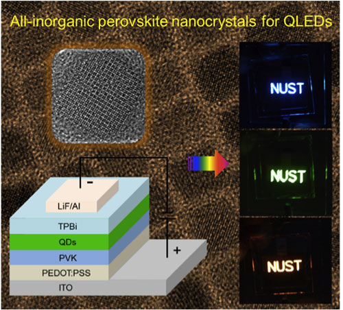
Now, researchers have presented a new family of photoelectric materials for light-emitting devices: colloidal all-inorganic perovskite cesium lead halide QDs. This new material could find applications in LEDs and lasers, and has an especially big potential in high-performance displays, lighting, monochromatic narrow-band photodetectors, and optical communications.
« We discovered that our newly engineered quantum dots possess superior optical gain properties, representing a new class of solution processed, low-threshold, truly stable and wavelength-tunable gain materials, » Professor Haibo Zeng, Director of the Institute of Optoelectronics & Nanomaterials at Nanjing University of Science and Technology. « The solution process ability of these QDs also makes them applicable for device fabrication from simple and cost-effective printing and spraying technologies. »
Découvrir