The main characteristic of Spark Plasma Sintering (SPS) is that the pulsed or unpulsed DC or AC current directly passes through the graphite die, as well as the powder compact, in case of conductive samples. Joule heating has been found to play a dominant role in the densification of powder compacts, which results in achieving near theoretical density at lower sintering temperature compared to conventional sintering techniques.
The heat generation is internal, in contrast to the conventional hot pressing, where the heat is provided by external heating elements. This facilitates a very high heating or cooling rate (up to 1000 K/min), hence the sintering process generally is very fast (within a few minutes). The general speed of the process ensures it has the potential of densifying powders with nanosize or nanostructure while avoiding coarsening which accompanies standard densification routes. This has made SPS a good method for preparation of a range of materials with enhanced magnetic, magnetoelectric, piezoelectric, thermoelectric, optical or biomedical properties.
SPS is also used for sintering of carbon nanotubes for development of field electron emission electrodes.
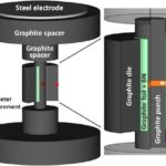
Functioning of SPS systems is schematically explained in the picture. While the term « spark plasma sintering » is commonly used, the term is misleading since neither a spark nor a plasma is present in the process. It has been experimentally verified that densification is facilitated by the use of a current. SPS can be used as a tool for the creation of functionally graded soft-magnetic materials and it is useful in accelerating the development of magnetic materials. It has been found that this process improves the oxidation resistance and wear resistance of sintered tungsten carbide composites compared to conventional consolidation methods.
Découvrir