Chemical Vapor Deposition (CVD) is a well-known technique in the nanofabrication space known for being able to take a vaporized reactant and deposit it onto a surface to form a thin film. There are many thin films and nanomaterials which can be fabricated using CVD, with the most notable being graphene. While graphene is the most widely known product of CVD, it can also be used to create thin film semiconductor materials, which is discussed in this article.
The use of semiconductors is growing around the world and they are now a staple material in some technologies—for example, solar cells—and their need is only going to grow as technology further advances. Many of the semiconductor materials that were first used were quite bulky, but as technology has started to become smaller and smaller, more advanced fabrication methods are being devised to make semiconductor thin films that can be utilized in these technologies, rather than bulkier semiconductor materials.
What is Chemical Vapor Deposition (CVD)?
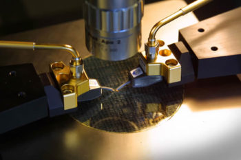
To understand how CVD can be used to create specific thin films, then it is best to first discuss what CVD is and how it works from a general perspective. CVD is known as a bottom-up nanofabrication technique as it builds a material from scratch, atom by atom by depositing and reacting the atoms on a surface (often a metal foil). CVD is a technique that typically uses a lot of heat during its process, but it is known to be quicker than many other nanofabrication techniques.
CVD is always performed under a vacuum. The process starts by feeding the reactants into the reactor before vaporizing them into a gas. This is often done using high temperatures or by a plasma (but other methods are used as well), and the way in which the heating or plasma formation is performed is the usual differentiator between the techniques. The atoms in the gas are then fed into the reaction chamber by an inert carrier gas where they are deposited onto the substrate present in the reaction chamber. The vaporized atoms then react and decompose on the surface of the substrate which creates a chemically bonded thin film on top of the substrate. The by-products of the reaction are then desorbed from the surface of the substrate and removed from the reactor.
Applying CVD to Semiconductor Thin Films
Now, CVD is useful for many monoatomic materials—such as graphene which is only made of carbon—but it can get more complex when it comes to semiconductor materials as they often contain either multiple metal atoms or metals with nitrogen atoms. The one example which is simpler is silicon, which is one of the earliest semiconductor materials known, and silicon thin films can be produced in a CVD reactor system from silane (SiH4). Silicon dioxide can also be produced by reacting the silane in the presence of oxygen.
Now, if you want to create more complex semiconductor thin films—such as gallium arsenide (GaAS) or gallium nitride (GaN)—then metalorganic CVD (MOCVD) is often used. It has now established itself as a way of growing complex crystalline layers on to a semiconducting wafer and has become one of the most popular methods for manufacturing III-V semiconductor materials. MOCVD is similar to conventional CVD and can be used to grow a number of layers of top of each other with varying compositions. The epitaxial layer growth of the layers is often controlled via the reactants for each layer alongside the manufacturing conditions.
Like many other CVD techniques, MOCVD is an extension and adapted version of CVD which uses highly pure heated gas flows (often hydrogen) into the reaction chamber. The main difference between MOCVD and other techniques is how the reactants are introduced, as they are often introduced via a bubbler. The bubbler works by passing the carrier gas through a heated metalorganic liquid, where the carrier gas picks up some of the metalorganic vapor atoms and transports them to the reaction chamber.
The key driver of MOCVD is that it can be used to deposit extra layers on top of a semiconducting wafer. The ability to create crystalline layers on top of the substrate is due to the reactions that occur between the organometallic atoms and hydride atoms that are involved in the reaction, as the layers which are created provide a surface to promote epitaxial growth where other layers can be bonded on top.
Discover