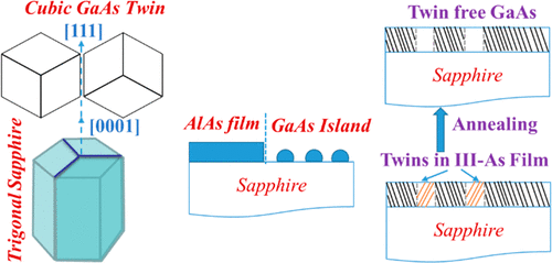
19 August 2019

[Thin films] – Crystalline GaAs Thin Film Growth on a c-Plane Sapphire Substrate

Home > News > [Thin films] – Crystalline GaAs Thin Film Growth on a c-Plane Sapphire Substrate
Flèche contenu
Crystalline AsGa thin film Growth - Codex International

Crystalline zinc blende GaAs has been grown on a trigonal c-plane sapphire substrate by molecular beam epitaxy. The initial stage of GaAs thin film growth has been investigated extensively in this paper. When grown on c-plane sapphire, it takes (111) crystal orientation with twinning as a major problem. Direct growth of GaAs on sapphire results in three-dimensional GaAs islands, almost 50% twin volume, and a weak in-plane correlation with the substrate. Introducing a thin AlAs nucleation layer results in complete wetting of the substrate, better in-plane correlation with the substrate, and reduced twinning to 16%. Further, we investigated the effect of growth temperature, pregrowth sapphire substrate surface treatment, and in-situ annealing on the quality of the GaAs epilayer. We have been able to reduce the twin volume below 2% and an X-ray diffraction rocking curve line width to 223 arcsec. A good quality GaAs on sapphire can result in the implementation of microwave photonic functionality on a photonic chip.

Discover Also
[Perovskites] – Perfecting perovskites – new gas-quench method yields more stable solar cells 24 January 2024

The new method of making mixed halide-perovskites results in solar cells with improved stability and performance. The new method results in better control over perovskite crystallization rates. This means the crystal structure is more ordered, in part due to researchers understanding and taking advantage of the faster crystallization of bromide relative to iodide.
The result is a material with fewer defects and less halide migration and thus less segregation of the bromide and iodide. This in turn means uniform mixing of bromide and iodide across the material, which allows the material to absorb light evenly. The end result is that solar cells made using the new method will perform better under real-world conditions.
Typical halide perovskite solution deposition uses an anti-solvent drip procedure to initiate crystallization of the halide film. The standard anti-solvent method for producing bromide-iodide mixed halide perovskite films often leads to excessive defect formation (e.g., bromide vacancies) owing to the rapid crystallization of bromide vs. iodide-perovskite phases. Simulations show that halide migration is enhanced in the presence of a large population of halide vacancies. This limits the stability of bromide-iodide mixed halide perovskites under light and heat.
In comparison to the anti-solvent approach, the gentler gas-quench method better controls crystallization, first producing a bromide-rich surface layer that then induces top-down columnar growth to form a gradient structure with less bromide in the bulk than in the surface region. The anti-solvent method does not produce such a gradient structure.
In this study, researchers from the National Renewable Energy Laboratory, the University of Toledo, and the University of Colorado Boulder demonstrated that the gas-quench method also produces fewer bromide vacancies and results in materials with a higher quality opto-electronic performance. Solar cells made using the gas-quench method retain desirable light absorption properties and provide enhanced performance in the form of a higher charge carrier mobility, higher open circuit voltage, and enhanced stability.

Read more
[Graphene] – Growing large-area single-grain graphene layers 16 February 2021

In the background material to his Nobel Prize talk in 2010, Prof. Geim illustrated the strength of graphene with his now famous cat hammock example : The unit hexagonal cell of graphene contains two carbon atoms and has an area of 0.052 nm2. That translates into a density of 0.77 mg/m2. A hypothetical hammock measuring one square meter made from graphene would thus weigh 0.77 mg.

Read more