Researchers can optimize the performance of multi-layered, post-fabricated organic photovoltaic devices doped with gold nanoparticles by using combined X-ray diffraction and X-ray fluorescence.
Context
One of the key elements of a sustainable energy future is the Photovoltaic (PV) cell. Today, there are numerous device architectures under development, aimed at maximizing the conversion of sunlight into electricity. While the best performing cells are made from silicon, the creation of organic polymer-based PV cells offers a cheap and mass producible alternative with a low environmental impact.
For an organic PV architecture to be considered highly promising, it must include a bulk heterojunction polymer made from nanoscale donor-acceptor blends. This is typically composed of a conjugated polymer and a soluble fullerene derivative. Thus, such devices have the potential to herald a technological revolution allowing flexible, transparent solar cells to be painted onto walls or windows, owing to the ease of chemical processing and the low-cost fabrication of thin films.
The Challenge
Organic PV cells are not as efficient as silicon PV cells. In fact, the efficiency of organic PV cells tends to decrease markedly over time. Thus, in order for such technologies to become mature enough for routine industrial production, there is a need for discovering novel solutions to harvest light more efficiently.
Here, with the introduction of metallic nanoparticles to the polymer layer, it is possible to enable localized surface plasmon resonances to strongly absorb light in the UV–visible band, thus enabling high performance and durable solar cells.
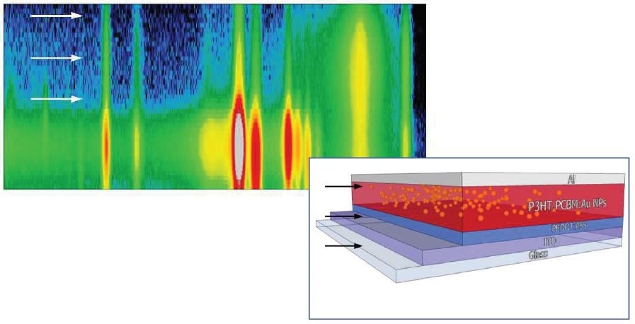
Researchers can now obtain detailed characterization of a post-fabricated multilayered organic electronic device coated with gold nanoparticles, thanks to combined vertical scanning X-ray diffraction and fluorescence spectroscopy at ESRF beamline ID11. To probe the sandwich-type geometry of organic photovoltaic cells, laboratory-based techniques alone are insufficient. However, the high penetration depth and small spot size of synchrotron X-rays facilitate changes in the nanoparticle distribution and structural properties of the organic layer to be monitored as a function of device depth.
The Results
This technique's accuracy makes it possible to measure the nanoparticle distribution profile across the device thickness. Moreover, in situ measurements are able to provide a space-resolved description of the molecular ordering of the polymer component of the photoactive layer. Since the rate of photovoltaic energy conversion is strongly dependent on the nanoscale phase separation during the donor/acceptor heterojunction formation, this information is crucial for developing higher performing solar cells. Further, the rate of photovoltaic energy conversion also depends on nanomorphology of the interfaces formed between the active and the charge-collecting layer.
The results of this experiment uncovered a number of underlying chemical-physical phenomena – including modification of the local nanostructure and organization, interface effects, and inter-diffusion processes – occurring due to the annealing process used to optimize organic solar cell efficiency.
Conclusion
Powerful in situ spatially resolved studies have highlighted the detailed structure of post-fabricated multilayered organic electronic devices, thus revealing underlying mechanisms that lead to the different organic layers and interfaces' structural properties.
Today, new insights have been achieved, revealing the role of plasmonic nanoparticles. This represents a major breakthrough towards a better understanding of the correlation between the performance of organic photovoltaic cells and the morphology of their respective components on the nanoscale.
Due to the high spatial resolution achieved at the ID11 beamline, the results discussed above represent a major milestone towards elucidating structure-property relations that link different length scales ranging from local nano/hetero-structures and interfaces to large-scale devices.
This technique can be used for any thin-film device and coating. What's more, upcoming advances in modern nanofocusing X-ray optics will enable detailed analyzes of virtually any type of multilayered organic electronic device on all relevant length scales.