Metalenses are ultrathin, flat surfaces that use nanostructures to focus light. They have attracted tremendous attention because they can overcome limitations of conventional bulky, curved and heavy refractive optical lenses and they are poised to revolutionize everything from microscopy to cameras, sensors, and displays.
Despite these advantages, mass production of these flat optics – for instance for waver-level devices – is still not possible due to the low productivity and high cost of electron beam lithography, which has been commonly used to make metalenses.
What is needed are printable and high-refractive index materials for the mass production of high-efficiency metalenses including general metasurfaces. However, so far there has been no material satisfying these requirements.
Researchers in Korea now have developed a high-throughput, scalable nanocomposite printing method to manufacture metalenses at low cost, paving the way to commercializing them.
The team has published their findings in ACS Nano (“Printable Nanocomposite Metalens for High- Contrast Near-Infrared Imaging”).In previous research, titanium dioxide (TiO2) or gallium nitride (GaN) have been used as suitable materials for high-efficiency metasurfaces. However, the fabrication – deposition and etching – of these materials is highly challenging and too expensive for commercialization.
“In contrast” as Prof. Junsuk Rho from Pohang University of Science & Technology (POSTECH), who led this work, explains to Nanowerk, “our nanocomposite material, which is also suitable for high-efficiency metasurfaces, can be molded into metalenses just by one step of printing without any secondary operations such as thin-film deposition or plasma etching.”
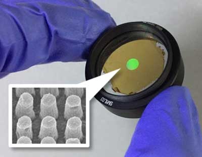
The researchers synthesized their nanocomposite by dispersing silicon nanoparticles in the matrix of UV-curable resin to achieve a high-refractive index to increase the efficiency of the metalenses. The printing mold is reusable, so the large-scale metalenses can be printed rapidly and repeatedly.The fabricated metalens shows a focusing efficiency of 47% at λ = 940 nm, and, according to the team, the efficiency can be further increased by optimizing the composition of the silicon nanocomposite.
Although silicon nanoparticles have been used as a key element of this nanocomposite, the team points out that there are still many kinds of nanoparticles – such as quantum dots and upconverting nanoparticles – that potentially could be used instead.
“The effects of these functional nanoparticles with metasurfaces has not been established yet, and we believe that it will be possible to discover new quantum-nanophotonic phenomena or develop novel nanophotonic devices such as nano-lasers,” says Rho.
He notes that the nanocomposite printing process demonstrated by his team can be applied to not only metalenses, but also general metasurfaces such as metaholograms, color filters, perfect absorbers and optical cloaks.Applying their nanocomposite printing technique, the researchers demonstrate a near-infrared (NIR) metalens, which can have applications in LiDAR sensors (receivers), IR cameras, CCTV, night vision devices and biometric devices such as vein recognition.
This printing method is also capable of realizing visible metalenses, and possible applications in this area include ultrathin optical camera modules (smartphones), compact DSLR camera lenses and many other optical devices using conventional optical lenses.
“There have been many attempts to correct various optical aberrations such as spherical aberration, chromatic aberration and coma by using just a single metalens,” says Rho. “Some of the precedent works have shown such promising possibility, but the design strategy has not been perfect. Therefore, we need to develop novel design principles for such aberration-free metalenses.”
“The biggest challenge facing future research in this field is that numerical simulation of metasurfaces is very time consuming,” he concludes. “Therefore, we need to develop novel approaches to designing metasurfaces; deep learning can be a promising candidate for this purpose.”
A team of researchers has discovered a new mechanism to stabilize the lithium metal electrode and electrolyte in lithium metal batteries. This new mechanism, which does not depend on the traditional kinetic approach, has potential to greatly enhance the energy density — the amount of energy stored relative to the weight or volume — of batteries.
Read moreThe main characteristic of Spark Plasma Sintering (SPS) is that the pulsed or unpulsed DC or AC current directly passes through the graphite die as well as the powder compact, in case of conductive samples.
Read more