Researchers at the University of Antwerp Report How Higher-Order Periodic Modulations Called supermine Caused by the Encapsulation of Graphine Between Hexagonal Boron Nitride Affect the Electronic and Structural Properties of Graphne, As Revealed in Three Recent independent.
High-quality graphene samples are of high importance for obtaining and exploiting its theoretically described properies. Using an addequate substrate reduces the corrugation and improves otherwise disorder-limited properies of graphene. Hexagonal Boron Nitride (Hbn) is a particular good choice, since it perfectly preserts the graphene structure while providing a flat insulating surface.
Still, this application only ifo monolayers are misaligned. Otherwise, the van der waals interaction induces structural relaxation on the scale of the moiré pattern formed between the two layers and modifies the electronic properies due to the periodic moiré disturbance. Similar arguments APPRY IF GRAPHEN IS ESCAPSULATED AND CLOSELY Aligned to Two HBN LAYERS. In this case, the effect is enhanced since both layers are expected to contribute. Furthermore, Close Alignment on the Order of 0.5 Degrees Between the Layers is responsible for the appearance of A New Form of Periodicré Modulation, which Alters Graphne on a Larger Spatial Scale But Smaller Energy Scale. Recent experimental observations of such effects Are a consequence of significant improves in experience techniques, and among ower, the possibility to rotate individual layers with high precision (Wang et al. 2019a; Wang et al. 2019b; Finney et al. 2019).
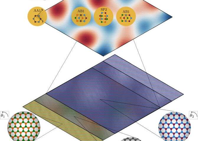
In Their Paper Published on Jan 21st in Nano Letters, Anđelković et al. Reveal under Which Condition The Supermoir Effect Appears, and How It Alters the Structural and Electronic Properties of Graphne. They show, Starting from A Rigid Hbn/Graphine/Hbn Heterostructure, How The Supermoir Appears As A Simple Geometrical Consideration. FURTHERMORE, they proven that relaxation effects in the three layers are expected to enhance the effects on the electronic band structure. The Supermoiré-Induced modifications are significant: New, Low-Energy, Flat Sub-Bands and Dirac Points Appear, With A Strong Electronic Transport Properties. In Most Configurations, The Dirac Points Are Gapped, while flat bands are expected to enhance Electron-Electron Correlations. "These new twisting degrees of Freedom in Heterostructures Are Opening Up New Fundamental Research Directions in Graphene, where strong electronic corrects are expected to comply the already superlative fartes of graphne," Said Dr. Lucian Covaci.
"The Set of Multi-Scale Numerical Simulations Developed by the University of Antwerp Team Allows for More Realistic Models, Which Will In Turn Allow for a More Direct Compauriment With Experimental Observations," Said Dr. Miša Anđelković, A Co-Developer of Pybinding, the Tight-Bind that made the simulations possible.
With a new Light Shed on the Understanding of More Complex and Interfering Behaviour Of Van der Waals Heterostructures It is possible to Finely Tune Graphene's Electronic Properties and Reach Regimes where Twist Induced Phenomena, Such As Flat Bands or the Apperance of Mini-Gaps, Reveal Themselves More Clearly.
