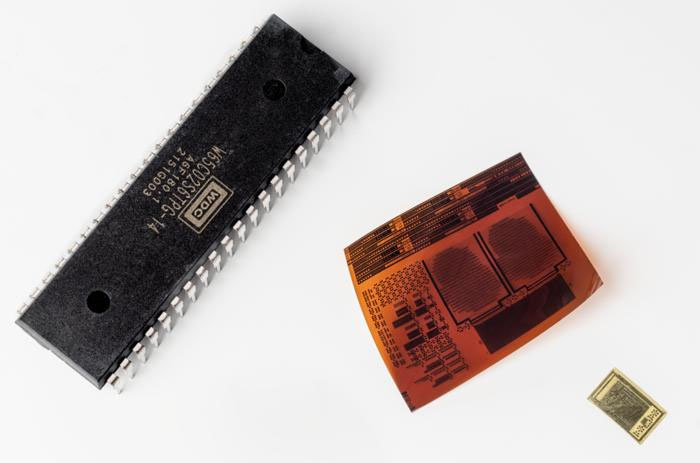
The mass production of conventional silicon chips relies on a successful business model with large ‘semiconductor fabrication plants’ or ‘foundries’. New research by KU Leuven and imec shows that this ‘foundry’ model can also be applied to the field of flexible, thin film electronics. Adopting this approach would give innovation in the field a huge boost.
The findings have been published in Nature (“Multi-project wafers for flexible thin-film electronics by independent foundries”).Silicon semiconductors have become the ‘oil’ of the computer age, which was also demonstrated recently by the chip shortage crisis. However, one of the disadvantages of conventional silicon chips is that they’re not mechanically flexible. On the other hand you have the field of flexible electronics, which is driven by an alternative semiconductor technology: the thin-film transistor, or TFT. The applications in which TFTs can be used are legion: from wearable healthcare patches and neuroprobes over digital microfluidics and robotic interfaces to bendable displays and Internet of Things (IoT) electronics.
TFT technology has well evolved, but unlike with conventional semiconductor technology the potential to use it in various applications has barely been exploited. In fact, TFTs are currently mainly mass-produced with the purpose of integrating them in displays of smartphones, laptops and smart TVs – where they are used to control pixels individually. This limits the freedom of chip designers who dream of using TFTs in flexible microchips and to come up with innovative, TFT-based applications.
“This field can benefit hugely from a foundry business model similar to that of the conventional chip industry”, says Kris Myny, professor at the KU Leuven’s Emerging technologies, Systems and Security unit in Diepenbeek, and also a guest professor at imec.
Foundry business model
At the heart of the worldwide microchip market is the so-called foundry model. In this business model, large ‘semiconductor fabrication plants’ or ‘foundries’ (like TSMC from Taiwan) focus on the mass production of chips on silicon wafers. These are then used by the foundries’ clients – the companies that design and order the chips – to integrate them in specific applications. Thanks to this business model, the latter companies have access to complex semiconductor manufacturing to design the chips they need.
Myny’s group has now shown that such a business model is also viable in the field of thin-film electronics. They designed a specific TFT-based microprocessor and let it be produced in two foundries, after which they tested it in their lab, with success. The same chip was produced in two versions, based on two separate TFT technologies (using different substrates) that are both mainstream.
Multi-project approach
The microprocessor Myny and his colleagues built is the iconic MOS 6502. Today this chip is a ‘museum piece’, but in the 70s it was the driver of the first Apple, Commodore and Nintendo computers. The group developed the 6502 chip on a wafer (using amorphous indium-gallium-zinc-oxide) and on a plate (using low-temperature polycrystalline silicon). In both cases the chips were manufactured on the substrate together with other chips, or ‘projects’. This ‘multi-project’ approach enables foundries to produce different chips on-demand from designers on single substrates.
The chip Myny’s group made is less than 30 micrometer thick, less than a human hair. That makes it ideal for, for example, medical applications like wearable patches. Such ultra-thin wearables can be used to make electrocardiograms or electromyograms, to study the condition of respectively the heart and muscles. They would feel just like a sticker, while patches with a silicon-based chip always feel knobbly.
Although the performance of the 6502 microprocessor is not comparable with modern ones, this research demonstrates that also flexible chips can be designed and produced in a multi-project approach, analogue to the way this happens in the conventional chip industry. Myny concludes: “We will not compete with silicon-based chips, we want to stimulate and accelerate innovation based on flexible, thin-film electronics.”
Researchers have long sought to maximize the efficiency of perovskite solar cells while minimizing production costs.
Read moreEvery age in the history of human civilisation has a signature material, from the Stone Age, to the Bronze and Iron Ages. We might even call today’s information-driven society the Silicon Age.
Since the 1960s, silicon nanostructures, the building-blocks of microchips, have supercharged the development of electronics, communications, manufacturing, medicine, and more.

