With the advancing of material science, nowadays the thin film deposition technology is developing quickly and has a crucial role in our everyday lives. Thin film deposition is the act of applying a thin film on the surface of another material. It is used in the manufacturing of devices such as computers and thin film transistors. It also finds applications in the production of semiconductors as well as in simple everyday objects as a typical household mirror.
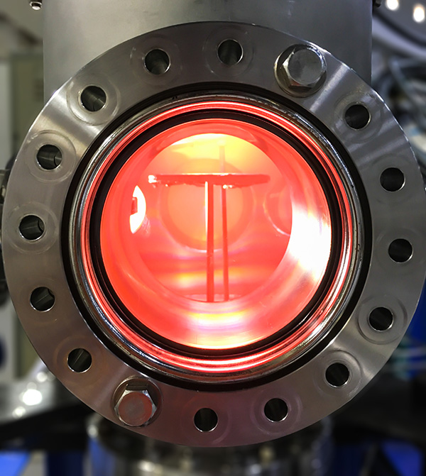
The deposition of thin films on a surface is used for modification of the physical or chemical properties of the surface of the coated material. They can change its optical, electrical and thermal properties; however, thin films do not change the bulk properties of the material. The process of creation of a deposit contains 3 basic steps – first, the depositing substance is synthesized, then it is transported from the substance to the surface of the material. Finally, it is deposited onto the substrate so a film is formed. If those three steps are independent of each other, the degree of flexibility of the process is increased as each step could be individually controlled and varied if needed. There are three types of techniques for thin-film deposition – purely physical, purely chemical and a mixed physical-chemical method.An example of a purely physical method is vacuum evaporation. To perform vacuum evaporation the source and the substrate are situated in an evacuated vacuum chamber with a heater inside. The source is heated until it starts evaporating and atoms and molecules will start leaving its surface. When the particles reach the surface of the substrate, they will condense onto it as it has a much lower temperature. There they will depose creating a film layer. The thickness of the layer depends on several different factors one of which is the evaporation rate from the source.
Gas-phase chemical processes, such as thermal oxidation, are examples of purely chemical deposition techniques. In thermal oxidation, the subtract itself provides the material to create the deposition layer. This process occurs at a temperature in the range of 700˚C to 1200˚C. One of the most important thermal oxidation methods is the one using silicon dioxide. Since silicon naturally forms stable oxides, the high temperature just helps accelerate the process. It is very important in the production of semiconductors and the manufacturing of silicon devices.
Examples of mixed physical-chemical methods are glow-discharge technologies. A glow discharge is a plasma created by a current which passes through a gas. In its simplest form, it consists of a cathode and anode in a cell which is held at low pressure (about 0.1-10 Torr). The most commonly used technique used in a glow discharge process is called sputtering. It occurs when atoms are ejected from an electrode surface due to ions colliding with the surface atoms. There are a few different sputtering processes – diode sputtering, reactive sputtering, ion-beam sputtering, bias sputtering and magnetron sputtering.
In the case where a DC diode is used, the two electrodes are placed in a vacuum chamber. The material to be sputtered is called a target. It is the cathode in the system – simply a plate that is held at negative potential and the substrate is the anode. The cathode is bombarded by positive ions and ejects atoms which are condensed onto the substrate. During the process, deposits are accumulated and a film is created on the anode. In reactive sputtering, the targets are placed in reactive gases such as ozone and carbon monoxide.
There are many other different ways to create thin-film deposition; however, it is important to always find the most suitable for specific needs. Some of the considerations that should be taken into account when choosing the particular are its specific applications and the physical and chemical properties of the materials that are to be used.
Découvrir