Carbon nanotubes (CNTs) that have been decorated with nanoparticles are effective biological and chemical sensors, photovoltaics, electronic conformal thermal interface substances, and surfaces for heterogeneous catalysis. The particle structure of the sidewalls of the CNT has an effect on the performance and properties of metal-nanotube hybrids for these types of applications.
Methods for Nanoparticle Decoration of Carbon Nanotubes
Nanoparticles are often deposited electrochemically, which generally require treatments that are time-consuming and contain strong acid for surface detection production. This acid can compromise the intrinsic mechanical or transport properties of the CNTs, restricting their multi-functionality. Alternative techniques to electrochemical treatment, such as vapor deposition, are undertaken to facilitate the growth of metal nanoparticles in situ on the multi-wall carbon nanotube (MWCNT) sidewalls.
Sputtering Process
This article discusses the analysis of the vapor phase growth of nickel, titanium, and gold nanoparticles on bulky paper MWCNTs. The inherent binding energy of elemental metals strongly influences the nanoparticle size and distribution, for example; the use of metals with large cohesive energies would result in the growth of nanoparticles with a smaller diameter and higher density.
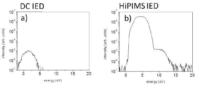
The use of energetic metal ions, characterized as illustrated in Figure 1, for in situ modification of the MWCNT surface during their growth could alter any metal nanoparticle diameter to mimic that of metals with different binding energies. The carbon atom removal from the surface of a MWCNT uses the kinetic energy of incident ions > 5-7 eV. The use of the sputtering process to control the ariel density, morphology, diameter of metal nanoparticles deposited on the sidewalls of as-received and annealed MWCNTs for nickel, titanium and gold was demonstrated.
Based on the defect density of the surfaces of MWCNTs and the parameters of intrinsic sputtering process (kinetic energy and metal ion flux in particular), it is possible to produce gold nanoparticles with an average diameter range of 5 – 30 nm. It is also possible to control the defect density of the MWCNT surfaces by annealing before the sputtering process. The characteristics of the nanoparticles can be modified with the total incident ion flux and temperature during processing, or with the initial diameters of the carbon nanotubes. The MWCNT diameter significantly influences the geometry of the nanoparticles.
Particle elongation along the axis of the nanotube was achieved for diameters of tube < 30 nm. Nanoparticles with a strong alignment along the axis of the nanotube were observed, especially for those MWCNTs with greater defect densities. Scaling up the PVD process, employed for nanoparticle growth for large arrays of CNTs, is possible. The PVD process will be studied to add multi-functionality properties to the nanocomposites, based on CNTs.
CVD is a well-known technique in the nanofabrication space known for being able to take a vaporized reactant and deposit it onto a surface to form a thin film. There are many thin films and nanomaterials which can be fabricated using CVD, with the most notable being graphene.
Lire la suiteScientists make extensive use of X-ray fluorescence to map elements in materials. However, this technique does not have the needed spatial sensitivity unless the probe is finely focused.
Scientists have now found a way to turn X-ray fluorescence into an ultra-high position-sensitive probe to measure tiny internal structures called nanostructures in thin films (Nature Communications, « Reconstruction of Evolving Nanostructures in Ultrathin Films with X-ray Waveguide Fluorescence Holography »).