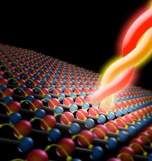
A special class of materials known as “Weyl semimetals” have unusual physical properties. In these materials, researchers can separate electrons by their “handedness.” That’s whether the electrons’ magnetic moment is in the same direction as the electrons’ movement or the opposite direction.
This results in a host of unique phenomena that researchers can use to turn infrared light into electricity and develop very fast electronic circuits.
In this research (Nature Materials, « Colossal mid-infrared bulk photovoltaic effect in a type-I Weyl semimetal »), scientists created devices based on one Weyl semimetal, tantalum arsenide. They observed that this material was able to convert more light to electricity than any other material. The conversion was 10 times higher than previous measurements with other materials.
The bulk photovoltaic effect is a way to convert light into electrical current. Scientists may be able to use this effect to increase efficiency and reduce costs compared to conventional approaches to solar cells.
In this research, scientists developed microscopic devices based on the Weyl semimetal tantalum arsenide. In most materials, the bulk photovoltaic effect is small.
However, the unique properties of Weyl semimetals led to the material demonstrating a much larger bulk photovoltaic effect than scientists have seen before. In addition, the photovoltaic devices they developed absorb mid-infrared light. This is an important wavelength for devices that conduct chemical and thermal imaging as well as waste heat recovery.
Scientists have observed a remarkably large mid-infrared bulk photovoltaic effect (BPVE) in microscopic devices made from the Weyl semimetal tantalum arsenide (TaAs). This discovery results from combining recent developments in Weyl semimetals, focused-ion beam fabrication, and theory, which suggested a connection between BPVE and topology.
First, the high efficiency of the nonlinear photovoltaic process comes from a unique property of Weyl semimetals where electrons can be separated by their chirality (“handedness”).
Second, previous research had shown that the photovoltaic response of these materials can be dominated by thermal effects.
In this study, scientists used a focused ion beam to fabricate a micrometer-scale slice of a TaAs crystal into an ideal shape for photovoltaic measurements. Then, combining a symmetry analysis with this device geometry enabled researchers to separate the shift current (photovoltaic effect) from photothermal effects.
The observed magnitude and wavelength range of the shift current advances our fundamental understanding of the effects of topology in materials. It also demonstrates the utility of Weyl semimetals for broad range of practical applications.
Source: Boston College
