Scientists from the Skoltech Center for Energy Science and Technology (CEST) and the Institute for Problems of Chemical Physics of Russian Academy of Sciences have developed a novel approach for preparing thin semiconductor fullerene films. The method enables fabrication of organic electronics without using toxic organic solvents and costly vacuum technologies, thus reducing the environmental risks and making organic electronics more accessible.
The results of their study were published in the Journal of Materials Chemistry C (« Environment-friendly aqueous processing of [60]fullerene semiconducting films for truly green organic electronics »).
Organic electronics provides manufacturers with unique capabilities inconceivable in other technologies. The light weight, flexibility and low cost of organic semiconductors along with their tailored through chemical modification properties opens wide opportunities for designing inexpensive and efficient devices for the Internet of Things (IoT) technology, real-time health monitoring, food quality control and many other applications.
However, there are several obstacles for wide-scale commercial use of organic semiconductors, in particular the environmental risks associated with mass production of organic semiconductor electronics using coating and printing techniques with a large volume of environmentally hazardous toxic organic solvent vapors discharged into the atmosphere.
The vacuum methods are environmentally friendly but very energy-intensive, which results in much higher production costs and larger emissions of CO2 and other greenhouse gases in energy generation.
Replacing toxic organic compounds, such as chloroform, toluene or 1,2-dichlorobenzene, with safe solvents like water or alcohols can be a major breakthrough.
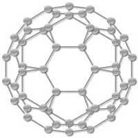
A unique form of carbon, fullerene C60, is represented by molecules similar in shape to a soccer ball and possessing a wealth of remarkable properties, in particular being good n-type semiconductor. However, like many other semiconductors, it is mostly soluble in toxic (and often chlorinated) organic solvents.
Earlier, a research team led by Skoltech Professor Pavel Troshin demonstrated that sulfur-containing fullerene derivatives decompose when slightly heated, producing initial fullerene. In their recent work, the researchers leveraged this property to obtain thin fullerene films from aqueous solutions.
« The goal of our study was to develop a method for coating thin films of fullerene from aqueous or alcohol solutions. Of particular interest in this context are sulfur-containing fullerene derivatives with ionogenic (amine or carboxylic) groups that are readily soluble in water.
This means that one can use aqueous solutions of these precursor compounds as « electronic ink » and apply them on a substrate using the existing printing and coating techniques to obtain the films that only need to be annealed to get a high-quality fullerene semiconductor films, » explains the first author of the paper and Skoltech PhD student, Artyom Novikov.
The fullerene semiconductor films obtained from a water-soluble precursor compound were used to make organic field-effect transistors with highly charge carrier mobility and gas sensors that can detect analyte (ammonia) in concentrations of less than 1 ppm.
The results obtained in this study feature a great potential of water-soluble precursor compounds for environmentally friendly production of organic electronics.
Source: Skolkovo Institute of Science and Technology (Skoltech)
