In its pristine/perfect atomic configuration, graphene is impermeable to all gases, even the tiniest airborne molecules, including helium (read more: World’s thinnest balloon made of graphene). However, pores in graphene (« defects ») can selectively allow the transport of gas and water molecules – which allows graphene to be tuned to enable selective permeability of gases.
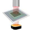
Usually, perfect single graphene crystals obtained by mechanical exfoliation are only of a few microns in size. However, practical applications require large area graphene, which is possible to synthesize by chemical vapor deposition (CVD) – but these larger sheets often come with defects and hence show high permeation rates.
Previous studies focused on clean transfer of monolayer graphene to form multi-stacked layers and sealing of graphene defects by polymers and atomic layer deposited (ALD) oxides. Barrier membranes based on (exfoliated) graphene or graphene oxide flakes inevitably have to be much thicker to compensate for the many possible permeation pathways, which negates at least part of the advantages (like transparency) that 2D materials can offer.
A new study by a team of UK researchers from the University of Cambridge; Centre for Process Innovation (CPI) Segdefield; and National Physical Laboratory (NPL) London have reported on improved performance of graphene-based moisture barrier layers. The research is published in the journal npj 2D Materials and Applications (« Graphene-based nanolaminates as ultra-high permeation barriers »).
« We have combined catalytic CVD and ALD to create in scalable fashion nanolaminates of few-layer graphene and aluminium oxide, » Dr. Abhay Sagade from the Department of Engineering at the University of Cambridge, and the paper’s first author, tells Nanowerk. « Unlike previous reports, this new approach exploits the synergy between different materials and growth techniques. »
The researchers point out that the ultra-thin (∼10 nm) graphene-based laminate films show excellent barrier performance over large areas (25 cm2) while maintaining high optical transparency (>90%) and flexibility.
« Importantly, this challenging task is accomplished by highly reliable measurements of low water vapor transfer rates (WVTR) below 7×10⁻³ g/m2 per day, utilizing not only optical Ca tests and OLED life time determination, but also in the ppb level traceability facility at NPL, » notes Sagade.
The team systematically benchmarked their results against the performance of existing state-of-the-art commercial multi-stacked barriers and industrially viable ALD aluminium oxide films and demonstrated that the nanolaminate films can be effectively integrated in organic light-emitting diodes (OLEDs), enabling half-life times of 880 hours in ambient.
They also demonstrated the usability of their nanolaminates as a potential material to be included in standard multi-stacked barrier layers to enhance the performance of existing ALD aluminium oxide and produce next generation moisture barriers.
« Our results highlight the potential of such heterogeneous material integration and the use of such nanolaminates as building block to engineer new functionalities and form factors for flexible and wearable technology, » concludes Sagade.