Researchers have reported a black phosphorus transistor that can be used as an alternative ultra-low power switch. A research team led by Professor Sungjae Cho in the KAIST Department of Physics developed a thickness-controlled black phosphorous tunnel field-effect transistor (TFET) that shows 10-times lower switching power consumption as well as 10,000-times lower standby power consumption than conventional complementary metal-oxide-semiconductor (CMOS) transistors.
The research team said they developed fast and low-power transistors that can replace conventional CMOS transistors. In particular, they solved problems that have degraded TFET operation speed and performance, paving the way to extend Moore's Law.
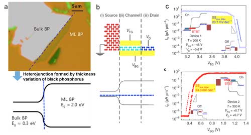
In the study featured in Nature Nanotechnology (“Thickness-controlled black phosphorus tunnel field-effect transistor for low-power switches”), Professor Cho's team reported a natural heterojunction TFET with spatially varying layer thickness in black phosphorous without interface problems. They achieve record-low average subthreshold swing values over 4-5 dec of current and record-high, on-state current, which allows the TFETs to operate as fast as conventional CMOS transistors with as much lower power consumption.
“We successfully developed the first transistor that achieved the essential criteria for fast, low-power switching. Our newly developed TFETs can replace CMOS transistors by solving a major issue regarding the performance degradation of TFETs,” Professor Cho said.
The continuous down-scaling of transistors has been the key to the successful development of current information technology. However, with Moore's Law reaching its limits due to the increased power consumption, the development of new alternative transistor designs has emerged as an urgent need.
Reducing both switching and standby power consumption while further scaling transistors requires overcoming the thermionic limit of subthreshold swing, which is defined as the required voltage per ten-fold current increase in the subthreshold region. In order to reduce both the switching and standby power of CMOS circuits, it is critical to reduce the subthreshold swing of the transistors.
However, there is fundamental subthreshold swing limit of 60 mV/dec in CMOS transistors, which originates from thermal carrier injection. The International Roadmap for Devices and Systems has already predicted that new device geometries with new materials beyond CMOS will be required to address transistor scaling challenges in the near future. In particular, TFETs have been suggested as a major alternative to CMOS transistors, since the subthreshold swing in TFETs can be substantially reduced below the thermionic limit of 60 mV/dec. TFETs operate via quantum tunneling, which does not limit subthreshold swing as in thermal injection of CMOS transistors.
In particular, heterojunction TFETs hold significant promise for delivering both low subthreshold swing and high on-state current. High on-current is essential for the fast operation of transistors since charging a device to on state takes a longer time with lower currents. Unlike theoretical expectations, previously developed heterojunction TFETs show 100-100,000x lower on-state current (100-100,000x slower operation speeds) than CMOS transistors due to interface problems in the heterojunction. This low operation speed impedes the replacement of CMOS transistors with low-power TFETs.
Professor Cho said, “We have demonstrated for the first time, to the best of our knowledge, TFET optimization for both fast and ultra-low-power operations, which is essential to replace CMOS transistors for low-power applications.” He said he is very delighted to extend Moore's Law, which may eventually affect almost every aspect of life and society.
Source: Korea Advanced Institute of Science and Technology