Perovskite solar cells have garnered widespread attention as a low-cost, high-efficiency alternative to conventional silicon photovoltaics. However, defects in perovskite films impede charge transport, resulting in energy loss and compromised operational stability.
One solution to this problem is “passivation treatment”—a process that adds chemicals such as simple salts or organic molecules to the film. These small molecules or ions latch onto defects in the perovskite material, preventing the defects from interfering with electrical flow.
Unfortunately, verifying the internal efficacy of various passivation treatments remains since most characterization techniques only probe challenging the surface or provide averaged macroscopic information.
Now, however, researchers at the Ningbo Institute of Materials Technology and Engineering (NIMTE) of the Chinese Academy of Sciences (CAS) have made an important breakthrough by developing a three-dimensional (3D) electrical imaging technique that directly reveals how defect passivation treatments work in perovskite films.
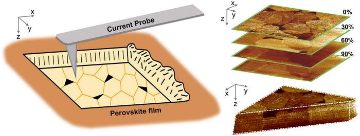
The technique employs tomographic conductive atomic force microscopy (TC-AFM) to visualize current distribution across perovskite films by sequentially stripping ultrathin layers of the film while measuring local electrical conductivity at varying depths. By stacking these measurements, a 3D map of charge transport within the film can be reconstructed with nanoscale resolution.
Using this approach, the researchers characterized the internal electrical behaviors of perovskite films treated with different passivation strategies. Untreated films exposed extensive low-conductivity regions that hindered charge transport. While bulk passivation significantly reduced these resistive areas within the film, particularly along grain boundaries.
In contrast, surface passivation primarily enhanced conductivity near the top interface—a critical factor for device integration. Importantly, they discovered that films treated with both bulk and surface passivation demonstrated the most uniform and continuous conductive pathways, with remaining low-conductivity regions largely confined to the surface.
“These microscopic electrical characteristics are closely correlated with the resulting solar cell performance, establishing a direct link between 3D charge transport within the film and overall device efficiency,” noted Prof. XIAO Chuanxiao, a corresponding author of the study.
By providing a direct, 3D view of charge-carrier migration through perovskite films, this work offers a powerful tool for evaluating and optimizing passivation strategies. The method pave the way for the rational design of higher-quality perovskite materials, enabling more efficient and stable perovskite solar cells while advancing a broad range of thin-film electronic and optoelectronic devices.