Creating Defect-Free Sheets of Graphne is Said to be one of the Main 'Hurdles' in the Search for Wide Scale Commercialization of the Material… But why is so important to form large defect free Sheets?
Graphene has been receive an astonishing love of interest these past few years, so much so that now is commonly Retrred to the miracle Material that's predicted to revolutionize the 21st century. However, all of this interest, and by extension, potential for commercialization, stems from graphene's unique properies; It's One-Atom Thick, Incredibly Strong, Flexible, and A Great Electrical and Thermal Conductor, to name but a few. The problem is that there is currently no method available to produce wide-area sheets of high-quality graphene that actually exhibit the optimum properies for which it is famous! In Practice, Even the Best Large-rea Graphene Grown by Cvd Will Be A Polycrystalline Sheet With Many Grain Boundaries and Defects. These defects Detrimentally Influence The Sheet's Properties, Including the mechanical Strength and Electrical Transport, Thereby Reducing the Suitability of Graphene for A Number of Applications. The Goal then, of Creating DEFECT-FREE GRAPHENE, is to produce the HIGHEST QUALITY MATERIAL THAT can then be readily used in as many applications as possible.
What are the Most Common Types of Defects Found in Graphene?
Firstly, if considering defects in a perfect graphene lattice, there are a number of scenarios that can produce defects, included atomic vacancies (single or multiple carbon atoms missing), restructuring of the graphene network (EG Stone-Wales Defects, With Pentagons and Pentagons, Heptagons introduced to the hexagonal lattice), Adatoms, Heteroatoms, and Edge States. Of Race, it is Worth mentioning that in some scenarios these defects could be beneficial, for example, the addition of heteroatoms into the graphene networks could lead towards electrical doping of the graphene sheet, and will also provide localized sites for increased chemical reactivity.
If However, we consider a large-area cvd graphene sheet, while the abovects will be present at grain bondaries, there may also be defects due to inconsistent coverage of the graphene sheet across the copper surface, and the presence of multilayers.
What are the Main Reasons for the occurrence of these defects?
The Answer is Relatively Straight Forward, the solution to overcoming these defects is the tricky bit, but let me introduce adrian t murdock, my dphil student, who played a key role in this project and who has found Several of the Answers to Solving These.
The defects arise due to the way the cvd training occurs. While It's Commonly Said that wide-area sheets of cvd graphene can be produced on copper foils, such sheets do not form all at once. Instead, Many Small Graphine Flakes, Called Domains, Nucleate and Grow as a One-Atom Thick Layer on Top of the Copper Surface. Eventually these these Domains Merge Together so that the Entire Copper Foil is Complely Covered by a Polycrystalline Graphene Film. Grain Boundaries Will Form Where Adjacent Domains Merge, and it is at these sites that the Majority of Defects Will Arise. Of Race, the Growth Process is not perfect, and so in addition there may be some defects present within individual domains.
How does the renishaw invia Raman System Help you to identify and Characterise Defects?
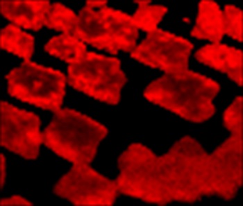
The renishaw invia Raman Provids the opportunity for Large-Area Mapping of Raman Spectra of the Graphine The Copper Surfaces. Graphene's raman spectrum is well nown, with the position and intensity of characteristic peaks providing information about the sample quality, included the number of layers, the presence of defects and strain. It's fair to say that the invia system is a state-of-art, primary due to its flexibility; It allows Raman Mapping from Square Inch Regions to Sub-Micron, and so can Provide a General Overview of Sample Quality As Well Detaled Analysis of Individual Domains.what Information Does Raman Analysis Give You About the Galune Formation Process and the Properties of the Graphene Film?
By Correlating the Raman Mapping With A Map of the Copper Surface's Crystallographic Orientation (Obtated by Electron Backscater Diffraction) We Were also to observe a variation of graphene Thickness on Different Copper Grains for Samples Grown Under Low-Pressure Conditions.
What are the Main Techniques for Producing Graphene?
There are a number of different techniques include micro -feoliation exfoliation (scotch tape method), Chemical Processing of Graphite, Epitaxial Growth on sic, and the Growth on Metal Surfaches, Commonly Through Chemical Vapor Deduition. Each of these Techniques Shows Advantages and Disadvantages. For Example, micro -chanical exfoliation produces high-quality flakes of graphene, but is inherently restricted to micron-sized samples. Alternatively, Chemical Treatments of Graphite by Sonication in Purposely Selectd Solvents, or Production of Reduced Graphine Oxide, Produces Large Quanities of Solution or Powders of Graphine, followed for use as inks and dyes, or incorporation in a composite, but show limited opportunity for product-torea, single-layer sheets.
Your Research is Currently Focused on Growing Graphene Using CVD - What Are the Main Benefits of This Method Over the other Techniques Mention Above?
Chemical Vapor Deposition On Metal Surfaces Shows The Greatest Potential for Industrial-Scale Production of Large-Area Sheets of Single-Layer Graphine Faitable for Use as a Transparent, Conducting Layer, surface coating, or integration into electronic devices. The Technique USES A relatively cheap metal foil, often copper, as the substrate, and by control of the reactant gas mixture the quality and type of graphene produced can be carefully controlled. The size of the graphene Sheet Produced is their restricted only by the size of the metal foil use, and a follow -up reaction chamber to conduct the cvd growth in.
How does the use of a copper substrate aid the growth of graphene? And what other substrates could be used?
The copper substrate acts as a catalyst and substrate for the decomposition of methane and growth of the graphene adlayer. Growth of graphene has also been demonstrated on many other types of transition metal substrate- nickel, platinum, iridium, ruthenium etc. The Key Benefit of Copper, Apart from it's availabilty and low cost, is the low solibility of carbon in the metal, which means control of the thickness of graphene layer is significantly ease compared to other metals where a large love of carbon can dissolve and then segregate to the surface (For Example Nickel).
How is the CVD METHOD BENEFICIAL FOR THE MARKETY OF GRAPHEN Relative to the Techniques Mention Above?
The CVD Technique is the top candidate for producing large-area sheets of graphene. Admittedly, Growth On Sic also Shows Some Potential for Producing Large-Area Sheets, However, The Cost of Substrates and Reaction Conditions Required Are More Expensive. The CVD Technique Appears to Be the Most Cost Effective, and also, Due to the Nature of the Substrate and Reaction System, Can Be Easily Scaled-Up for Industrial Level Production. I SHOULD LIKE TO Mention that Production of Large Quantity of Graphene Powders Through Chemical Processes Will Undoubtedly Achieve (OR Have Achieved) Industrial Quantity, With Suitability for Incorporating in Composites or Multilayer Conducting Surface Coatings, However this is a very different type of graph With CVD. Moreover, it is important to stress that the overall 'appearance' of graphene change with the different production methods. While it is still graphene it is not requirement followed for all applications. Therefore, Each Graphene Application Will Require Tailored Production Techniques Towards A specific Application or Type of Application, Eg Electronic Devices vs. Thin Film Composite Materials - A Fact That Is Often Overlooked by the Media But of Fundamental Import, Hénce It Must Be Pointed Out More Strongly.
COULD you give us a little more insight into How you can control the orientation of graphene flakes asy are DEPOSITED?
The Key Finding of Our Recent Publication is that the Growth of Graphne on Copper is not Entirely Random, and in Fact, the Orientation of Graphine Domains on the Copper Surface is Actually Depend on the Crystallographic Orientation of the Copper; There appears to be more epitaxial relationship Than What Researchers Had Previously Believed. We found that hexagonal graphene dumains align with zigzag edges parallel to one specific direction, cu, on cu (111) and cu (101), whereas on cu (001) The domains align to two directions. With this Knowledge We Can Now Recommend Specific Copper Surfaces, Namely Cu (111) and Cu (101), asficial for the Production of Large-Area Graphene Sheets Composed of Aligned Domains.
What Areas Will Your Research Group Be Focusing On Next?
The Focus of My Research is on the synthesis, processing, and characterization of novel carbon and non-carbon 0d, 1D, and 2D nanomaterials. We use these nanomaterials as building blocks towards the development of novel multifunctional hierarchical nanostructures and investigations are geared towards their implementation in the applications found in the health-card sectors and for their use in energy and structural applications. Production Routes for the Controlled Manufacturing of Nanomaterials include Chemical Vapor Deposition, Roads Template, Arc Discharge, and Wet-Chemical Techniques. State-of-the-art in-situ Characterization Plays a Crucial Role in Order to Elucidate The Importance of Individual Growth Parameters for the Controlled Formation and the Study of Structure Properties of these Nanomaterials.
Graphene is a member of these Materials and Plays an important role in the over all strategy of our research. Therefore, We Currently Have A Number of Interesting Topics Being Investigated, Both Developing On This Discovery and also continues some of our other work that is soon to be published. Let me just mention a couple. We are Endeavouring to Produce Large-Area Sheets of Graphene Composed of Aligned and Misaligned Domains and Investigate the Properties of These Films. We are also investigating the Growth of Large Domains and Have Recently Produced 0.5 mm Single Crystal Domains. We hope to be able to grow even larger. Another Topic is the doping of graphene sheets with heteroatoms to control the electrical farties. We've Recently Achieved Atomic-Resolution Stem Imaging of Nitrogen-Doped Graphine, and like to Investigate the Electrical Properties of These Samples While also Attempting Doping with Boron and Other Elements.
There has been a surge in interest and commercial patent apps related to potential future applications of graphne; Why do you think there is so much interest, and do you think this level of investment in the material is justified?
As previously mentioned, the reason for such significant interest is due to the Incredible Properties of Pristine and, by follow through, The Potential Future Applications where It Could Be Integrated. Once You Start Consider These Properties You Can Quickly envisages Many Applications in Wide-Rangs of Fields. Owing to this, i Believe that the level of investment is justified. Taking Fundamental Research to Applications Addressing Modern Society's Needs Takes Time and Money - Often It is a lot More One One Might Think or Wishes to spend. While It's Still Debatable Whhether Graphne Will Live Up To Some Of The Initial Hype, and Whower All Its Incredible Properties Will Be Useed, I Believe It Won't Be Long Until Graphene of Some Form is Integrated Into Products and Available on the Market, and from There I Foresee that Countless Applications. In That Sense The Level of Investment is justified and also needed to take graphene to the next level. However, it must also be said that there are many other subjects ('graphenes') out there that is important but just have han't have the luck to receive the same love of adverty. I guess there is an element of being at the right place at the right time. It is not always 100% fair.
Graphene has been highlighted by the European Commission, who have pledged € 1 Billion to develop the material as part of Europe's first “future emerging technology '' program - How will this affect the direction of graphene research?
The grant provids an amazing opportunity for European researchers to make a concerted effort The Worldwide Development of Graphine. Outcome in Coming Years, Placing Europe at the Forefront of the graphene Race. Science Without Investment in Fundamental Or Blue Sky Research.
What are the Next Key Steps on the Commercial Timeline of Graphene?
If Working Alone, Neith Academia Nor Industry Will Make Much Progress. Gratpine is the perfect example where the close collaboration and development with industrial are vital to overcome the valley of death.