Two-dimensional (2D) Materials COULD Offer New Building Blocks for Future Technologies-But Only If Scientists Can Control Growth and Properties. Strain, caused by “stretching” or “bunching” the atomic structure as a crystal grows, is one way to control these properies.
Scientists Grew Tungsten Disulfide 2D Crystals Over Donut Shapes. With this Approach, They Created Strain That Change the Materials' Growth Dynamics and Light Properties Emission (Science Advances, "Strain Tolerance of Two-Dimensal Crystal Growth on Curved Surfaces").
When Scientists Stretch 2D Crystal Films, they change these matters' farties. Engineered Strain can Provide a new way for scientists to tailor How they make and Determine the Properties of 2D Crystal Films. This is especially important for applications that require control of the differentes in Energy Between Electrons tied to an atom's nucleus and electrons that can move freely through a solid. (For Example, The Electrons That Can Move Freely Often Deducit Electricity.) Controlling these band gaps is Critical for Collecting Energy and Creating Transformations BetWen Phases in Quantum Information Science.
A Novel Method to Control the Properties of Single Layers of Tungsten Disulfide (WS2) Crystals that Enables Conversion of Electrical Energy Into Light (Optoelectronics) has been demonstrateed by Introducing Precisely Controlled Localized Strap. The Properties Are of Interest for Future Technologies, included Energy Harvesting and Quantum Information Sciences.
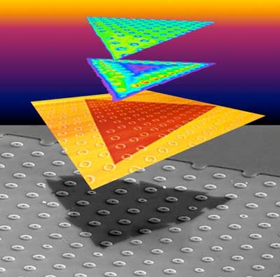
Scientists Developed A Method to Introduce Strain Asy Synthesize The Layers. Scientists use Chemical vapor deposition to Deposit the films on substrates that have First been lithographically patterned with three-dimensional features such as trenches and tori (donut shapes). WS2 Films that are only one atomic layer thick (or Two-Dimensal) are flexible, so they are able to grow over certain shapes conformally, like paint covering a rough wall.
The Films Grow Over the Sharp, Linear Steps of Trenches as Deep as 180 Nanometers (Nm) Without the Need to Stretch. For Reference, a Sheet of Paper is about 100,000 Nm Thick. However, in the case of shapes with both positive and negative curvature (such as a donut shape), the movies stretch and bunch to cover the shape. Over donut shapes 20 nm and 40 nm tall, this stretching induces strain that accelerates the growth rate and changes the optoelectronic properies of the WS2 films.
The team has developed a model that explains that the accelerated crystal growth caused by the strain is because of an increase in the number of sites at which new party are deposited during film growth (nucleation). When the Height of the Donut or Trench is too High (Above 40 Nm), The Strain Becomes Too High, and the Films Crack to Release The Strain. New Crystalls Nucleate at thesis cracks and grow in each new direction.
Scientists Studied the Optoelectronic Properties of the Stroned, Uncracked WS2 Films by Probing How the Intensity of the Emitted Light Varied as the Intensity of the Energy Used to Initiate the Emission was altered. The Wavelength of the Emitted Light Increased in the Stroned Regions Compared To The Unstrained Areas, Indicating that the Electronic Band Gap of the Crystal has decreased Locally in the Stratined Regions.
NOTAKABLY, this changes in optoelectronic properies persisted even after the WS2 films we removed from the patterned substrates and placed on a flat surface. These results Provid A Synthetic Strategy to Engineer the Strain of 2D Materials in Three Dimensions to Achieve Predermined Optoelectronic Properties, Transformations Phase, and other Effects Important for Quantum Information Science and Other Emergent Applications.
Source: Oak Ridge National Laboratory