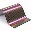
While efficiency is a primary concern for solar cells, researchers have also focused on developing solar cells that are lightweight, low-cost, and flexible. However, the fabrication process itself has posed a serious environmental concern: the use of toxic materials and generation of industrial waste.
For instance, copper indium gallium selenide (CIGSe) is a thin-film solar cell that offers several advantages over traditional silicon solar cells. Thin-film solar cells are about 100 times thinner, cheaper to make, and are easier to install on rooftops and vehicles.
Moreover, compared to other photovoltaic materials used in thin-film solar cells like amorphous silicon, cadmium-telluride, and organic materials, CIGSe absorbs light more strongly and can be prepared into thinner films.
However, they contain a buffer layer of cadmium sulfide, which is highly toxic and carcinogenic. This makes finding alternative, non-toxic materials essential for large-scale production and installation of CIGSe panels.
For Professors Jakapan Chantana and Takashi Minemoto at Ritsumeikan University, Japan, removing cadmium from solar cells was as important as developing an eco-friendly manufacturing process that is both efficient and affordable. Addressing these issues in a new study (Solar RRL, « Formation of Native Inx(O,S)y Buffer through Surface Oxidation of Cu(In,Ga)(S,Se)2 Absorber for Significantly Enhanced Conversion Efficiency of Flexible and Cd-Free Solar Cell by All-Dry Process »), a research team led by them developed a strategy in which the traditional cadmium sulfide buffer layer was replaced with a native buffer layer formed by oxidizing the surface of the Cu(In,Ga)(S,Se)2 CIGSSe layer with an air-annealing process.
While attempts to oxidize the CIGSSe layer have been made before, the surface usually takes months to oxidize. With the new method, however, the team reduced the oxidation time to a few hours, allowing for a faster manufacturing by a “roll-to-roll” process.
In this process, a CIGSSe layer is initially deposited on a flexible stainless-steel substrate. The deposition is then followed by an air-annealing process where the surface of the CIGSSe layer is oxidized to form native buffer layers of Inx(O,S)y.
By experimenting with different oxidation conditions, the researchers fabricated a CIGSSe solar cell with a maximum energy conversion efficiency of 16.7% after 6 hours of oxidation at 130 °C.
“We have disclosed for the first time that the CIGSSe surface oxidized through an optimized air-annealing process leads to a strong enhancement in energy conversion efficiency,” says Prof. Minemoto.
Although the reported efficiency is lower than that of conventional solar cells (which typically exceed 20%), the developed method manages to do away with cadmium, making the solar cells eco-friendly.
“In the conventional process, cadmium is deposited on the CIGSSe layer via a chemical bath deposition process. By eliminating this step, we have created a completely dry manufacturing process that generates less waste,” explains Prof. Chantana. Moreover, the process is also cost-effective.
In order to make solar energy a viable source of clean energy, solar panels must become more efficient, economical, and eco-friendly.
“The method developed in our study can be scaled to large-scale manufacturing applications, which is what we need to make solar cells a clean energy resource not only in Japan but all over the world,” concludes Prof. Minemoto.
Découvrir