Drs. Chaun Jang, Jun Woo Choi, and Hyejin Ryu of the Korea Institute of Science and Technology (KIST, President Lee Byung Gwon) have announced that their team at KIST’s Center for Spintronics successfully controlled the magnetic properties of FGT (Fe3GeTe2) in a joint research project with Dr. Se Young Park and his team at the Center for Correlated Electron Systems at the Institute for Basic Science (IBS).
Fe3GeTe2 has recently attracted attention as a material for next-generation spintronic semiconductors.
Named by combining the terms spin and electronics, spintronics is a new field in electronic engineering that aims to replace conventional silicon semiconductors by utilizing electron spin, a quantum property of electrons.
Van der Waals materials, also known as two-dimensional (2D) materials, are layered materials composed of planes that are attached to each other via a weak van der Waals interaction. These include various materials such as graphene and molybdenum disulfide. When combined with other 2D materials, they can create new materials that show previously undiscovered properties. This is why 2D materials, which have a variety of properties, such as superconductivity, semi-conductivity, and metallicity have been the subject of so many studies.
In 2017, 2D van der Waals materials that show magnetic properties were discovered, stimulating research projects and studies all around the world.
However, most van der Waals magnetic materials have some constraints in terms of spintronics application because of their low Curie temperature (a transition temperature point where a ferromagnetic material changes to a paramagnetic one or vice versa) and high coercivity (the intensity of magnetic field required to reduce the magnetic flux density of a ferromagnetic material to zero after the magnetism of that material has been saturated), making them unsuitable for use in certain devices.
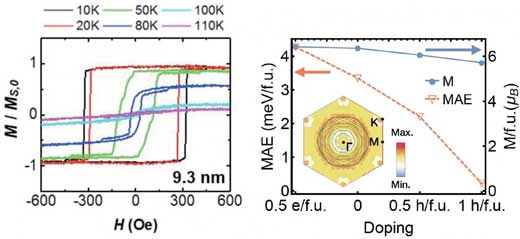
A number of studies have been done on FGT, a recently discovered van der Waals material with a layered structure. The joint KIST-IBS research team discovered an efficient scheme for controlling the properties of FGT.
The team conducted an experiment in which they observed the material while controlling the number of electrons, leading them to discover changes in the properties of FGT. The team proved that the magnetic anisotropy (This refers to the directional dependence of a material’s magnetic properties on a crystallographic or geometric structure. Depending on such structures, a material can have easy or hard magnetization directions), which describes how the material’s magnetic properties change depending on the direction, contributed to such changes.
The research results (Nano Letters, « Controlling the Magnetic Anisotropy of the van der Waals Ferromagnet Fe3GeTe2 through Hole Doping ») revealed the origin of the changes in the FGT magnetic properties, thus presenting a possible method of efficiently controlling the properties of 2D magnetic materials.
Furthermore, the research team announced that by potentially controlling the properties of single-atom-thick van der Waals magnetic materials, the development of spintronic devices which operate 100-times faster than current silicon-based electronic device, could be accelerated.
Dr. Hyejin Ryu of KIST said, « We started this study to discover the magnetic properties of van der Waals materials and apply such properties to spintronic devices. » She added, « Further development of new materials for semiconductors with various properties will be possible through the use of van der Waals magnetic materials and other van der Waals materials based heterostructures. »
Source: Korea Institute of Science and Technology