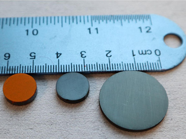
Perovskite, a family of materials with unique electric properties, show promise for use in a variety fields, including next-generation solar cells. A Penn State-led team of scientists created a new process to fabricate large perovskite devices that is more cost- and time-effective than previously possible and that they said may accelerate future materials discovery.
“This method we developed allows us to easily create very large bulk samples within several minutes, rather than days or weeks using traditional methods,” said Luyao Zheng, a postdoctoral researcher in the Department of Materials Science at Penn State and lead author on the study. “And our materials are high quality — their properties can compete with single-crystal perovskites.”
The researchers used a sintering method called the electrical and mechanical field-assisted sintering technique (EM-FAST) to create the devices. Sintering is a commonly used process to compress fine powders into a solid mass of material using heat and pressure.
A typical process for making perovskites involves wet chemistry — the materials are liquefied in a solvent solution and then solidified into thin films. These materials have excellent properties, but the approach is expensive and inefficient for creating large perovskites and the solvents used may be toxic, the scientists said.
“Our technique is the best of both worlds,” said Bed Poudel, a researcher professor at Penn State and a co-author. “We get single-crystal-like properties, and we don’t have to worry about size limitations or any contamination or yield of toxic materials.”
Because it uses dry materials, the EM-FAST technique opens the door to include new dopants, ingredients added to tailor device properties, that are not compatible with the wet chemistry used to make thin films, potentially accelerating the discovery of new materials, the scientists said.
“This opens up possibilities to design and develop new classes of materials, including better thermoelectric and solar materials, as well as X- and γ-ray detectors,” said Amin Nozariasbmarz, assistant research professor at Penn State and a co-author. “Some of the applications are things we already know, but because this is a new technique to make new halide perovskite materials with controlled properties, structures, and compositions, maybe there is room in the future for new breakthroughs to come from that.”
In addition, the new process allows for layered materials — one powder underneath another — to create designer compositions. In the future, manufactures could design specific devices and then directly print them from dry powders, the scientists said.
“We anticipate this FAST perovskite would open another dimension for high throughput material synthesis, future manufacturing directly printing devices from powder and accelerating the material discovery of new perovskite compositions,” said Kai Wang, an assistant research professor at Penn State and a co-author.
EM-FAST, also known as spark plasma sintering, involves applying electric current and pressure to powders to create new materials. The process has a 100% yield — all the raw ingredients go into the final device, as opposed to 20 to 30% in solution-based processing.
The technique produced perovskite materials at .2 inch per minute, allowing scientists to create quickly create large devices that maintained high performance in laboratory tests.
The team reported their findings in the journal Nature Communications (« A universal all-solid synthesis for high throughput production of halide perovskite »).
Penn State scientists have long used EM-FAST to create thermoelectric devices. This work represents the first attempt to create perovskite materials with the technique, the scientists said.
“Because of the background we have, we were talking and thought we could change some parameters and try this with perovskites,” Nozariasbmarz said. “And it just opened a door to a new world. This paper is a link to that door — to new materials and new properties.”
Other Penn State researchers on the project were Wenjie Li and Dong Yang, assistant research professors; Ke Wang, staff scientist in the Materials Research Institute; Jungjin Yoon, Tao Ye and Yu Zhang, postdoctoral researchers; Yuchen Hou, doctoral candidate; and Shashank Priya, former associate vice president for research and director of strategic initiatives and professor of materials science and engineering.
