The word « lens » takes its name from the Latin word for lentil. Both are both hemispheric shapes bound together on their flat surface. So a « flat lens » sounds like a contradiction of terms. Yet that is exactly what Andrei Faraon is working on at California Institute of Technology’s Nanoscale and Quantum Optics Lab.
Why flat lenses? They could be used in lots of places where conventional optical lenses are too bulky, Faraon, a member of the Kavli Nanoscience Institute at Caltech, explained. Built onto semiconductor sensors, surgeons could attach them to guide surgical tools and researchers could use them in microscopes designed to look at transparent objects inside cells.
There are several reasons conventional optical lenses fall short for these and other applications. Those lenses work by bending light, so it focuses on a single point in the center. Yet the curves used to gather light make conventional lenses expensive to manufacture. They also distort colors and produce less sharp images on their edges. To correct for those flaws, optical systems use additional lenses, which makes them bulky and more expensive.
Finally, in today’s digital world, engineers must couple those lenses with a separate image sensor, which makes them even bulkier and more costly.
Faraon thought he had a clear solution: Build a flat lens using the same techniques used to fabricate silicon semiconductor image sensors so that the lens and sensor form a small, single integrated system.
But first, he had to find a way to collect and focus light using a flat surface.
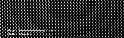
That’s what metasurfaces do. They are surfaces made of conventional materials–in this case, silicon–shaped into nanosized structures that alter how those materials respond to light. The most famous example of an optical metamaterial is a cloak developed at Duke University that bends light and makes objects appear invisible.
Faraon’s metasurfaces are dotted with 600-nanometer-high silicon cylinders that alters the path and speed of light as it passes through them. (Light always moves the same speed in a vacuum, but slows down when it passes through a medium like water or silicon.)
« As the light propagates through the pillars, it works like a convex lens, » he said. « The pillars in the center are fatter, so they delay light slightly longer than the thinner pillars on the edge. »
Through careful calculations, Faraon’s team designed an array of pillars that brought all light together on top of a flat image sensor like those used in smartphones and digital cameras.
At first, the metasurfaces produced images that were blurry around the edges. So, Faraon’s group borrowed a trick used by conventional lenses and put two metasurfaces on top of one another (with the nanopillars on the outside).
This enabled him to create a lens that gathered light from a 70-degree viewing angle and focused it crisply on a single plane. Faraon has also made flat telephoto lenses that zoom in on an image.
The lenses should also be easy to mass produce at reasonable cost, since they are made by the same silicon semiconductor technology used to make conventional image sensors.
« If you know what to do, it’s a simple to design compared with the design that goes into a computer processor, » Faraon said.
Yet flat lenses have one major shortcoming: they work for one wavelength of light only. If a camera with a flat lens took a picture of an outdoor scene, all that would show up on the image is a specific wavelength of red, blue, or another color.
Surprisingly, this is not a deal breaker. After all, lasers and LED lights also emit only a single wavelength of light. So, any application that uses a laser or LED to illuminate something could use a flat lens to gather light reflected from that object.
That makes them ideal for surgical instruments like endoscopes. These are long, thin rods with cameras and LED lights at the end, which doctors insert into body cavities and organs to perform minimally invasive surgery.
Coupled with infrared LEDs, it could be used as night vision cameras for security systems.
Another possible use lies in differential phase contrast imaging, a technique often used to look at transparent objects, like cells, organelles inside cells, and crystals. It uses very small differences in the speed at which light, usually from an LED, passes these objects to enhance the edge of the sample.
Faraon is already working on several of these applications, proving that a flat lens is not really a contradiction in terms.
Source: Kavli Foundation
Subscribe to a free copy of one of our daily
Nanowerk Newsletter Email Digests
with a compilation of all of the day’s news.
These articles might interest you as well:
Research News
(click here for Business News)
Scientists develop new method to isolate atomic sheets and create new materials
Feb 20, 2020
MoS nanoparticles provide a cheaper way to obtain hydrogen
Feb 20, 2020
New graphene-based metasurface capable of independent amplitude and phase control of light
Feb 20, 2020
In acoustic waves, engineers break reciprocity with ‘spacetime-varying metamaterials’
Feb 20, 2020
Plant-based relatives of cholesterol could give boost to nanoparticle gene therapy
Feb 20, 2020
Smart contact lens has potential to improve sight for many
Feb 19, 2020
A green chemistry preparation of fullerene films
Feb 19, 2020
Cellulose nanomaterials could make renewable energy cheaper
Feb 19, 2020
New world record for the conversion of solar energy to electricity using quantum dots
Feb 19, 2020
An early warning system for damage in composite materials
Feb 19, 2020
Improving the electrical and mechanical properties of carbon-nanotube-based fibers
Feb 19, 2020
Time-resolved measurement in a memory device
Feb 19, 2020
Topological materials outperform through quantum periodic motion
Feb 18, 2020
Highly sensitive sensors show promise in enhancing human touch
Feb 18, 2020
Ultrasound device improves charge time and run time in lithium batteries
Feb 18, 2020
Supersensitive nanomaterials for DNA diagnostics and targeted drug delivery
Feb 18, 2020
Flat lens gets ahead of the optical curve
Feb 18, 2020
Creating custom light using 2D materials
Feb 18, 2020
Power sources for smart contact lenses
Feb 18, 2020
Air-powered generator creates electricity ‘out of thin air’
Feb 17, 2020
Fast-charging, long-running, bendy graphene energy storage breakthrough
Feb 17, 2020
The origins of roughness
Feb 17, 2020
Light moves spins around
Feb 17, 2020
New nanocatalyst recycles greenhouse gases into fuel and hydrogen gas
Feb 17, 2020
Van der Waals magnets, a material for future semiconductors
Feb 16, 2020
Does graphene cause or prevent the corrosion of copper? New study settles the debate
Feb 15, 2020
Scientists propose new properties in hollow multishell structure
Feb 14, 2020
Ultrafast switching of an optical bit
Feb 14, 2020
Catalyst deposition on fragile chips
Feb 14, 2020
Skyrmions like it hot: Spin structures are controllable even at high temperatures
Feb 13, 2020
…more nanotechnology research news
Home|Privacy|Cookies|Terms of use|Contact us | What is Nanotechnology?|Sitemap|Advertise|Submit news
The contents of this site are copyright ©2020 Nanowerk. All Rights Reserved
This website uses cookies to improve service and provide ads. By using this site, you agree to this use. AcceptLearn more
Lasers are essential to many fields – ranging from optical communications and remote sensing, to manufacturing and medicine. While the semiconductor laser was first demonstrated nearly 60 years ago, advances in diode lasers and access to semiconductor fabrication techniques have enabled continued innovation and miniaturization of the technology.
Lire la suiteThin-film optics is the branch of optics that focuses on thin, structured layers of different materials. These layers range from a fraction of a nanometer up to several micrometers thick but are usually in the order of the wavelengths of ultraviolet light, which is about 500nm. Their synthesis is controlled via deposition, with one or more layers of material layered onto the substrate, usually via physical vapor deposition.
Lire la suite