Physicists at the University of Groningen have now imaged hydrogen at the titanium/titanium hydride interface with the help of a transmission electron microscope.
They successfully visualized both the metal and the hydrogen atoms in a single image by employing a new method. They were able to test various theoretical models describing the interface structure. The study outcomes were reported in the January 31st issue of the Science Advances journal.
Visualizing the structure of materials at an atomic resolution is generally crucial to gain insights into their properties. Although it is possible to use a transmission electron microscope (TEM) to visualize atoms, thus far, researchers have not been successful in generating accurate images of heavy atoms and hydrogen atoms, the lightest one of all, together.
Bart Kooi, Professor of Nanostructured Materials at the University of Groningen, and his team have now achieved this. A new TEM with capabilities that enable generating images of both hydrogen and titanium atoms at the titanium/titanium hydride interface was used.
Hydrogen Atoms
The ensuing images illustrate that hydrogen atoms occupy the spaces between the titanium atoms, thereby deforming the crystal structure. In accordance with previous predictions, the hydrogen atoms fill half of the spaces.
In the 1980s, three different models were proposed for the position of hydrogen at the metal/metal hydride interface. We were now able to see for ourselves which model was correct.
Bart Kooi, Professor of Nanostructured Materials, University of Groningen
Kooi and his team created the metal/metal hydride interface by beginning with titanium crystals. Then, atomic hydrogen was infused, which penetrated into the titanium in very thin wedges, thereby forming minuscule metal hydride crystals.
In these wedges, the numbers of hydrogen and titanium atoms are the same. The penetration of hydrogen creates a high pressure inside the crystal. The very thin hydride plates cause hydrogen embrittlement in metals, for example inside nuclear reactors.
Bart Kooi, Professor of Nanostructured Materials, University of Groningen
Related Stories
Hydrogen Storage Tanks For Use In Hydrogen Powered Motor Vehicles May Be Made Viable Using Nanotechnology
Determining the Hydrogen Adsorption Capacity of Porous Materials
Scientists Find New Way of Releasing Hydrogen from Fuel Cells by Using Ammonia Borane Compound
The escaping of hydrogen atoms is prevented by the pressure at the interface.
Innovations
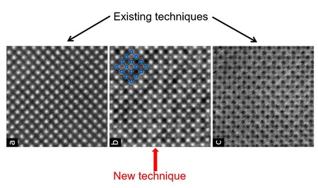
It was highly difficult to generate the images of the light hydrogen atoms at the interface and the heavy titanium. Initially, hydrogen was loaded into the sample. Then, it is essential to view it in a particular orientation along the interface. The researchers realized this by using an ion beam to cut accurately aligned crystals from titanium and making the samples thinner—to a thickness not exceeding 50 nm—again with the help of an ion beam.
A number of novel features added in the TEM enabled visualizing both titanium and hydrogen atoms. Visualization of heavy atoms can be performed using the scattering of the electrons they produce in the microscope beam. High-angle detectors are ideally used to detect the scattered electrons.
“Hydrogen is too light to cause this scattering, so for these atoms we have to rely on constructing the image from low-angle scattering, which includes electron waves.” But the material induces interference of these waves, due to which, thus far, it has been virtually impossible to identify the hydrogen atoms.
Computer Simulations
A low-angle, bright-field detector is used to detect the waves. The new microscope includes a circular bright-field detector split into four segments. The interferences can be filtered out and the very light hydrogen atoms can be visualized by studying the variations in the wavefronts found in opposing segments and by analyzing the differences that arise when the scanning beam crosses the material.
The first requirement is to have a microscope that can scan with an electron beam that is smaller than the distance between the atoms. It is subsequently the combination of the segmented bright field detector and the analytical software that makes visualization possible.
Bart Kooi, Professor of Nanostructured Materials, University of Groningen
Kooi worked closely with researchers from Thermo Fisher Scientific, manufacturer of the microscope. Two of the researchers are co-authors on the paper.
Different noise filters were added to the software by Kooi and his colleagues. These filters were then tested. Wide-scale computer simulations were also performed, and the experimental images were compared against these simulations.
Nanomaterials
The research demonstrates the interaction between the metal and the hydrogen, which is a vital understanding to investigate materials that can store hydrogen. “Metal hydrides can store more hydrogen per volume than liquid hydrogen.”
Moreover, it is also possible to apply the methods employed to image the hydrogen to other light atoms like nitrogen, oxygen, or boron, which are crucial in various nanomaterials. “Being able to see light atoms next to heavy ones opens up all kinds of opportunities.”
Researchers from the University of Rostock and Technion Haifa have created the first three-dimensional topological insulator for light. A judiciously placed screw dislocation allows optical signals to wind around the surface of a synthetic lattice while keeping it protected from scattering.
Their discovery has recently been published in the journal Nature (« Photonic topological insulator induced by a dislocation in three dimensions »).
Every age in the history of human civilisation has a signature material, from the Stone Age, to the Bronze and Iron Ages. We might even call today’s information-driven society the Silicon Age.
Since the 1960s, silicon nanostructures, the building-blocks of microchips, have supercharged the development of electronics, communications, manufacturing, medicine, and more.