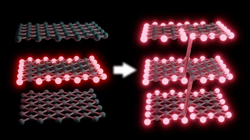
Researchers from the University of Rostock and Technion Haifa have created the first three-dimensional topological insulator for light. A judiciously placed screw dislocation allows optical signals to wind around the surface of a synthetic lattice while keeping it protected from scattering.
Their discovery has recently been published in the journal Nature (« Photonic topological insulator induced by a dislocation in three dimensions »).
Crystals have enthralled humans for thousands of years with their visual beauty and elegant symmetrical shapes, and, more recently, with their numerous technological applications. Fundamentally, these materials are based on a highly regular arrangement their smallest constituent elements, and the physical properties of crystalline materials depend strongly on the purity of their underlying lattice.
Yet, imperfections are not necessarily detrimental. For example, a sprinkling of atoms from adjacent groups in the periodic table is able to turn otherwise inert slabs of crystalline silicon into powerful electronic processors routinely carrying out billions of operations per second, as well as highly efficient solar cells capable of harvesting sunlight to power them.
As it turns out, the concept of discrete systems is not limited to solids, since the same underlying mathematical framework also describes the evolution of light in lattices of so-called waveguides. These ‘wires for light’ have fascinated Prof. Alexander Szameit of the University of Rostock for a long time.
“Every child knows that light travels in straight lines. At best, it can be reflected off a mirror or deflected by some angle as it enters a block of glass or passes through a lens,” the head of the solid-state optics group outlines the day-to-day experience with optics. “It never ceases to amaze me that light can actually be pinned to, and tunnel between, specific trajectories like electrons in a crystal,” he continues to describe the basis of his group’s research.
In this vein, arrays of waveguides can mirror many facets of solid-state physics, and even give rise to entirely new effects and novel functional structures.
For their newest breakthrough, the Rostock physicists teamed up with colleagues from Technion Haifa (Israel) and Zhejiang University (China) to construct a hitherto elusive artificial optical material: A three-dimensional topological insulator (TI) for light.
“Topological insulators are a new phase of matter and have only been known for a couple of decades,” author Dr. Lukas Maczewsky sketches the background of this work. “Their photonic counterparts can guide light around defects and sharp corners, and protect it from being scattered in the process.”
Yet, light moves at incredible speeds, and conventional photonic platforms typically have to sacrifice at least one of the three spatial dimensions to control the behavior of light in the remaining ones. Consequently, previous experiments on photonic TIs were restricted to one-dimensional and planar arrangements.
The elegant solution that the team of researchers came up with to overcome these limitations combines the concept of synthetic dimensions with a specific type of defect – a so-called ‘screw dislocation’. This judiciously placed defect continuously connects the individual planes of the lattice by twisting them around a central axis similar to a corkscrew.
Co-author and Ph.D. student Julius Beck explains: “Like transforming a loose stack of rings into a seamlessly connected spiral, this intentional defect allowed us to create the first 3D topological insulator for light.”
Carried out in the context of Rostock University’s recently established collaborative research center “LiMatI”, this successful international collaboration has substantially advanced fundamental research on topological photonics. While formidable challenges remain until these insights will find their way into consumer products, the physicists’ newest development has great potential for a wide range of innovative applications such as compact three-dimensional topological circuitry for light and a new class of functionalized optical materials with tailored properties.
Découvrir