Single-wall carbon nanotubes (SWCNT) have found many uses in electronics and new touch screen devices. Carbon nanotubes are sheets of one atom-thick layer of graphene rolled up seamlessly into different sizes and shapes. To be able to use them in commercial products like transparent transistors for phone screens, researchers need to be able to easily test nanotubes for their materials properties, and the new method helps with this.
Professor Esko I. Kauppinen’s group at Aalto has years of experience in making carbon nanotubes for electronic applications. The team’s unique method uses aerosols of metal catalysts and gasses containing carbon. This aerosol-based method allows the researchers to carefully control the nanotube structure directly.
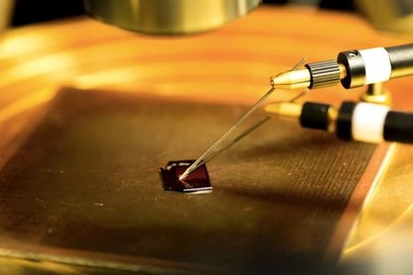
Fabricating single carbon nanotube transistors is usually tedious. It often takes days from raw carbon nanotube material to transistors, and the devices were contaminated with processing chemicals, degrading their performance. However the new method makes it possible to fabricate hundreds of individual carbon nanotube devices within 3 hours, an over ten times increase in efficiency.
Most importantly, these fabricated devices do not contain degrading processing chemicals on their surface. These so-called ultra-clean devices have been previously even more difficult to manufacture than regular single carbon nanotube transistors.
‘These clean devices help us to measure the intrinsic material properties. And the large number of devices helps to get a more systematic understanding of the nanomaterials, rather than just a few data points.’ says Dr. Nan Wei, a postdoctoral researcher in the group.
This study shows the aerosol-based nanotubes are superb in terms of their electronic quality, their ability to conduct electricity is almost as good as theoretically possible for SWCNTs.
More importantly, the new method can also contribute to applied research. One example is that by studying the conducting property of SWCNT bundle transistors, scientists may find ways to improve performance of flexible conductive films. This could prove useful for designers trying to build flexible, smash-proof phones. Follow-up work by the groups in Japan and Finland is already underway.
DécouvrirAlloys that can return to their original structure after being deformed have a so-called shape memory. This phenomenon and the resulting forces are used in many mechanical actuating systems, for example in generators or hydraulic pumps. However, it has not been possible to use this shape-memory effect at a small nanoscale: Objects made of shape-memory alloy can only change back to their original shape if they are larger than around 50 nanometers.
Lire la suiteBiosensors integrated into smartphones, smart watches, and other gadgets are about to become a reality. In a paper featured on the cover of the January issue of Sensors (« Vertically Coupled Plasmonic Racetrack Ring Resonator for Biosensor Applications »), researchers from the Moscow Institute of Physics and Technology describe a way to increase the sensitivity of biological detectors to the point where they can be used in mobile and wearable devices. The study was supported by the Russian Science Foundation.
Lire la suite