Light-emitting semiconductors are used throughout everyday life in TVs, smartphones, and lighting. However, many technical barriers remain in developing environmentally friendly semiconductor materials. In particular, nanoscale semiconductors that are tens of thousands of times smaller than the width of a human hair (about 100,000 nanometers) are theoretically capable of emitting bright light, yet in practice have suffered from extremely weak emission. KAIST researchers have now developed a new surface-control technology that overcomes this limitation (Journal of the American Chemical Society, « Overcoming the Luminescence Efficiency Limitations of InP Magic-Sized Clusters »).
A research team led by Professor Himchan Cho of the Department of Materials Science and Engineering has developed a fundamental technology to control, at the atomic level, the surface of indium phosphide (InP) magic-sized clusters (MSCs)—nanoscale semiconductor particles regarded as next-generation eco-friendly semiconductor materials.
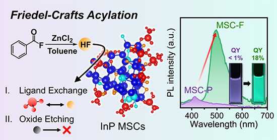
The material studied by the team is known as a magic-sized cluster, an ultrasmall semiconductor particle composed of only several tens of atoms. Because all particles have identical size and structure, these materials are theoretically capable of emitting extremely sharp and pure light. However, due to their extremely small size of just 1–2 nanometers, even minute surface defects cause most of the emitted light to be lost. As a result, luminescence efficiency has remained below 1% to date.
Previously, this issue was addressed by etching the surface with strong chemicals such as hydrofluoric acid (HF). However, the overly aggressive reactions often damaged the semiconductor itself.
Professor Cho’s team adopted a different approach. Instead of removing the surface all at once, they devised a precision etching strategy that allows chemical reactions to proceed in a highly controlled, incremental manner. This enabled selective removal of only the defect sites that hindered light emission, while preserving the overall structure of the semiconductor. During this defect-removal process, fluorine generated by the reaction combined with zinc species in the solution to form zinc chloride, which in turn stabilized and passivated the exposed nanocrystal surface.
As a result, the research team increased the luminescence efficiency of the semiconductor from below 1% to 18.1%. This represents the highest reported performance to date among indium phosphide–based ultrasmall nanosemiconductors, corresponding to an 18-fold increase in brightness.
This study is particularly significant in that it demonstrates, for the first time, that the surfaces of ultrasmall semiconductors—previously considered nearly impossible to control—can be precisely engineered at the atomic level. The technology is expected to find applications not only in next-generation displays, but also in advanced fields such as quantum communication and infrared sensing.
Professor Himchan Cho explained, “This work is not simply about making brighter semiconductors, but about demonstrating how critical atomic-level surface control is for achieving desired performance.”
