Biosensors integrated into smartphones, smart watches, and other gadgets are about to become a reality. In a paper featured on the cover of the January issue of Sensors (« Vertically Coupled Plasmonic Racetrack Ring Resonator for Biosensor Applications »), researchers from the Moscow Institute of Physics and Technology describe a way to increase the sensitivity of biological detectors to the point where they can be used in mobile and wearable devices. The study was supported by the Russian Science Foundation.
A biosensor is an electrochemical device that determines the composition of biological fluids in real- time. Blood glucose meters used by diabetic patients may well be the only mass-market biosensing devices in use today. But futurologists say household appliances will soon be able to analyze sweat, saliva, aqueous humor, and other bodily fluids to identify a person, make medical tests, diagnose disease, or continuously monitor the health of an individual and make optimal diet suggestions accordingly.
Until recently, such applications were not seriously considered, because the available devices were not sensitive enough and were prohibitively expensive for the consumer market. However, it may be that a breakthrough is about to happen. A team of researchers from the MIPT Center for Photonics and 2D Materials has proposed a radically new biosensor design, which could increase detector sensitivity many times over and offer a similarly impressive reduction in price.
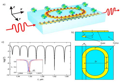
“A conventional biosensor incorporates a ring resonator and a waveguide positioned in the same plane,” explained MIPT graduate student Kirill Voronin from the Laboratory of Nanooptics and Plasmonics, who came up with the idea used in the study. “We decided to separate the two elements and put them in two different planes, with the ring above the waveguide.”
The reason researchers did not test that sensor layout before is that manufacturing a flat, single-level device is easier in a laboratory setting. By depositing a thin film and etching it, both a ring resonator and a waveguide are produced at the same time. The alternative two-level design is less convenient for manufacturing unique experimental devices, but it turned out cheaper for mass-producing sensors. The reason for this is that the technological processes at an electronics plant are geared toward layer-by-layer active component placement.
More importantly, the new two-tier biosensor design resulted in a many times higher sensitivity.
A biosensor operates by registering the slight changes in the refractive index at its surface, which are caused by organic molecule adsorption. These variations are detected via a resonator whose resonance conditions depend on the refractive index of the external medium. Since even the slightest fluctuations in the refractive index cause a significant resonant peak shift, a biosensor responds to nearly every molecule that lands on its surface.
“We have positioned the strip waveguide under the resonator, in the bulk dielectric,” said paper co-author Aleksey Arsenin, a leading researcher at the MIPT Laboratory of Nanooptics and Plasmonics. “The resonator, in turn, is at the interface between the dielectric substrate and the external environment. By optimizing the refractive indices of the two surrounding media, we achieve a significantly higher sensitivity.”
The newly proposed biosensor layout has both the source and the detector of light within the dielectric. The only part that remains on the outside is the sensitive element. That is, the gold ring several dozen micrometers in diameter and one-thousandth that in thickness.
According to Voronin, the team’s method for making biosensors more responsive will take the technology to a qualitatively new level. “The new layout is intended to make biosensors much easier to manufacture, and therefore cheaper,” the physicist said. “Optical lithography is the only technique necessary to produce detectors based on our principle. No moving parts are involved, and a tunable laser operating in a tight frequency range will suffice.”
Valentyn Volkov, who heads the MIPT Center for Photonics and 2D Materials, estimates that it will take about three years to develop an industrial design based on the proposed technology.
Source: Moscow Institute of Physics and Technology
