Borophene is the name for atomically thin, two-dimensional (2D) sheets of boron. Whereas boron is a nonmetallic semiconductor in its bulk form, it becomes a metallic conductor in 2D, even at a thickness of only one atomic layer.
Borophene is structurally similar to graphene, with a hexagonal network made of boron (instead of carbon) atoms on each of the six vertices defining the hexagon. However, borophene is different in that it periodically has an extra boron atom in the center of the hexagon.
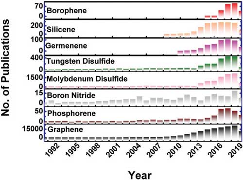
Since the 2004 discovery of graphene, scientists have been on the hunt for other 2D materials with remarkable properties. Numerous 2D materials have been synthesized or theoretically predicted, for example silicene and germanene, phosphorene, transition metal dichalcogenides, arsenene and antimonene.
Theorists predicted that boron (next to carbon on the Periodic Table, with one less electron) could be a 2D material similar to graphene. But this prediction was not experimentally confirmed until 2015, when scientists synthesized borophene on a silver substrate for the very first time. And in 2019, researchers finally managed to synthesize freestanding borophene sheets via sonochemical exfoliation.
Numerous experimental and theoretical studies of the mechanical properties, electronic structure, lattice thermal conductivity, superconducting properties, optical properties, atomic adsorption, and surface reactivity of borophene have shown its uniqueness.
A recent review of the state of borophene research (Advanced Materials, « Borophene: New Sensation in Flatland ») discusses various growth techniques and application areas for borophene and provides an in-depth summary of the material’s electronic, optical, thermal, and elastic properties compared to its 2D cousins.
Among 2D materials, borophene has attracted considerable attention owing to its unique chemical structure and impressive electronic conductivity and surface properties. As the authors point out, « apart from the usual covalent bonding, boron can form a three-center two-electron bonding, which enables the formation of a considerable number of atomic clusters having various sizes and atomic bindings. »
Graphene, the first discovered 2D material, is semimetallic, phosphorene is semiconducting, while borophene is metallic.
Freestanding borophene’s unique properties make it suitable for a wide range of applications in sensing, catalysis, energy conversion (fuel cells and supercapacitors), and energy storage.
Another intriguing feature of borophene is its atomic configuration. Borophene has two planar atomic sheet configurations: one of them is perfectly flat, referred to as X3 phase, while β12 is an atomic sheet having atomic ridges.
Unlike graphene, which is structurally isotropic in nature, the β12 phase of borophene is anisotropic and that in turn is expected to exhibit higher carrier density and mechanical stiffness in preferred direction.
In anisotropic materials, their mechanical or electronic properties – like their electrical conductivity – vary with different crystallographic orientations. In contrast, the properties of an isotropic material like graphene are the same in all directions.
The atomic ridges in β12 borophene provide higher electron densities along them. The spaces between the ridgelines can act as channels for ion transport in energy storage applications. The atomic binding of gaseous molecules on a borophene surface is expected to be better on the ridgeline as it can provide an enhanced anchoring.
Similarly, increased catalytic activities are expected. The unique properties and high potential for technological applications make borophene a promising material. However, further studies on its structural characteristics and properties are required before it can be commercialized.
Wrapping up their review, the authors conclude that borophene has progressed from conception to realization and is extensively studied for practical applications. It could be employed as a replacement for graphene in several applications such as terahertz applications and strengthening of plastics.
« As graphene has pushed the boundaries of science and engineering and changed the industries, borophene, lighter with abundant electrons, compared to graphene, would be a new cutting-edge material in the near future. The progress on borophene has been outstanding, but its high potentials are yet to be utilized. Borophene is a unique material with intriguing bonding capabilities and unprecedented physical and chemical behaviors for various instant and long-term applications. »
The rapid development of advanced nano-electronic technologies has prompted research into smart electronic skins (E-skins) that effectively mimic the distinctive features of the human dermis.
Lire la suiteEvery age in the history of human civilisation has a signature material, from the Stone Age, to the Bronze and Iron Ages. We might even call today’s information-driven society the Silicon Age.
Since the 1960s, silicon nanostructures, the building-blocks of microchips, have supercharged the development of electronics, communications, manufacturing, medicine, and more.