New graphene-based metasurface capable of independent amplitude and phase control of light
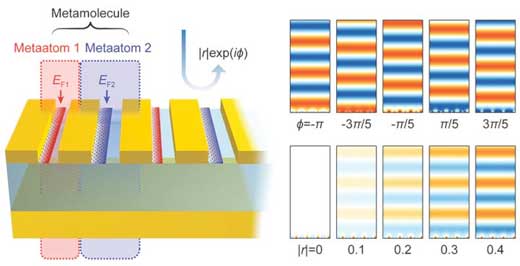
Researchers described a new strategy of designing metamolecules that incorporates two independently controllable subwavelength meta-atoms. This two-parametric control of the metamolecule secures the complete control of both amplitude and the phase of light.
A KAIST research team in collaboration with the University of Wisconsin-Madison theoretically suggested a graphene-based active metasurface capable of independent amplitude and phase control of mid-infrared light.
This research (« Complete Complex Amplitude Modulation with Electronically Tunable Graphene Plasmonic Metamolecules ») gives a new insight into modulating the mid-infrared wavefront with high resolution by solving the problem of the independent control of light amplitude and phase, which has remained a long-standing challenge.
Light modulation technology is essential for developing future optical devices such as holography, high-resolution imaging, and optical communication systems. Liquid crystals and a microelectromechanical system (MEMS) have previously been utilized to modulate light. However, both methods suffer from significantly limited driving speeds and unit pixel sizes larger than the diffraction limit, which consequently prevent their integration into photonic systems.
The metasurface platform is considered a strong candidate for the next generation of light modulation technology. Metasurfaces have optical properties that natural materials cannot have, and can overcome the limitations of conventional optical systems, such as forming a high-resolution image beyond the diffraction limit. In particular, the active metasurface is regarded as a technology with a wide range of applications due to its tunable optical characteristics with an electrical signal.
However, the previous active metasurfaces suffered from the inevitable correlation between light amplitude control and phase control. This problem is caused by the modulation mechanism of conventional metasurfaces. Conventional metasurfaces have been designed such that a metaatom only has one resonance condition, but a single resonant design inherently lacks the degrees of freedom to independently control the amplitude and phase of light.
The research team made a metaunit by combining two independently controllable metaatoms, dramatically improving the modulation range of active metasurfaces. The proposed metasurface can control the amplitude and phase of the mid-infrared light independently with a resolution beyond the diffraction limit, thus allowing complete control of the optical wavefront.
The research team theoretically confirmed the performance of the proposed active metasurface and the possibility of wavefront shaping using this design method. Furthermore, they developed an analytical method that can approximate the optical properties of metasurfaces without complex electromagnetic simulations. This analytical platform proposes a more intuitive and comprehensively applicable metasurface design guideline.
The proposed technology is expected to enable accurate wavefront shaping with a much higher spatial resolution than existing wavefront shaping technologies, which will be applied to active optical systems such as mid-infrared holography, high-speed beam steering devices that can be applied for LiDAR, and variable focus infrared lenses.
Professor Min Seok Jang commented, « This study showed the independent control amplitude and phase of light, which has been a long-standing quest in light modulator technology. The development of optical devices using complex wavefront control is expected to become more active in the future. »
Source: The Korea Advanced Institute of Science and Technology (KAIST)