In the background material to his Nobel Prize talk in 2010, Prof. Geim illustrated the strength of graphene with his now famous cat hammock example (taken from: Scientific Background on the Nobel Prize in Physics 2010 – Graphene): The unit hexagonal cell of graphene contains two carbon atoms and has an area of 0.052 nm2. That translates into a density of 0.77 mg/m2. A hypothetical hammock measuring one square meter made from graphene would thus weigh 0.77 mg.
In this 1 m2 graphene hammock tied between two trees you could place a weight of 4 kg before it would break. It should therefore be possible to make an almost invisible hammock out of single-layer graphene that could hold a cat without breaking. The hammock would weigh less that than 1 mg, corresponding to the weight of one of the cat’s whiskers.
« Though very engaging, this picture skips the fact that so far nobody has been able to produce such a large contiguous piece of graphene without grains and stitching, » Slava V. Rotkin, Frontier Professor of Engineering Science & Mechanics and Professor of Biomedical Engineering at the Materials Research Institute and Department of Engineering Science & Mechanics, The Pennsylvania State University, tells Nanowerk. « Our work shows that a method exists to produce such a perfect hexagonal net of atoms without stitching faults. We found that Nature organizes itself in a way to promote, under certain conditions, ‘knitting’ such an ideal lattice. »
In their paper in Advanced Materials (« Large-Area Single-Crystal Graphene via Self-Organization at the Macroscale »), Rotkin and a team of international collaborators demonstrate that single-grain growth of graphene crystals can be achieved over a large, macroscale, area (the team used a 5×5 mm substrate).
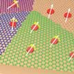
Specifically, the team shows that graphene flakes, nucleated over a polycrystalline graphene film, synchronize during growth so as to ultimately yield a common crystal orientation at the macroscale.
The phenomenon of self-alignment of graphene grains during their growth, which the team discovered experimentally, has never been observed before – and at this time the scientists don’t have a good model for the underlying physics which leads to this effect.
In their experiments, the team found that graphene islands self-align over large areas; later they proved that it was not just a ‘large’ area – the whole sample got involved in this correlated growth.
They then performed a lot of detailed studies to prove the effect and understand the details.
« We had a unique group to get it done, » says Rotkin. « Prof. Mark Rümmeli at Suzhou University and Dr. Huy Ta Quang at IFW Dresden are masters of CVD synthesis and, at the same time, world-leading experts in high-quality electron microscopy – while I was responsible in our team for theory and optical characterization. In order to discover the effect, we had to combine methods that are rarely used together: optical Raman microscopy and DF-TEM of the same sample. The challenge was to verify the single atom-thick islands’ orientation over an enormously large area. »
« When I saw coherent orientation of the islands for the first time, this was amazing – similar to the order appearing in large flocks of birds, » Rotkin points out. « Of course we are now keen to uncover the physics behind this phenomenon. »
A new scattering Scanning Near-field Optical Microscope – a $1M piece of equipment has been acquired recently in Rotkin’s lab at Penn State. “This customized instrument is set for nanoscale optical characterization – which will be the best tool for such atomistic studies at a large scale. »
For instance, scientists want to determine the forces between grains just as they form during the synthesis phase.
In the past, single-grain growth of graphene has been achieved by other methods, but they all require expensive substrates or quite complicated technologies. Devising a robust and inexpensive growth technique for large-area crystals has direct technological consequences for producing high-quality graphene.
« In all modern electronic devices, that have already reached atomic size limit, the variability is a major concern, » says Rotkin. « If industry will be able to produce high-quality graphene, with no grains, no stacking faults, and no misorientation, this would make the ‘wonder-material’ acceptable for use in commercial products and even desirable for a large number of technologies – from RF electronics to flexible displays. »
Rotkin concludes on a more cautionary note that the tasks of scaling up this technique to wafer-scale, translating it to other 2D materials, and being able to achieve full control of the crystal orientation might well take several years of research.