Negative differential resistance (NDR), which describes a decrease in electrical current as the applied bias increases, has always been one of the hottest topics in solid-state electronic devices since L. Esaki first demonstrated this phenomenon in heavily-doped Ge p−n junctions in 1958.
In recent years, along with the booming development of two-dimensional (2D) layered materials, there have been varieties of 2D van der Waals heterostructures that exhibit NDR characteristics, such as Esaki diodes made of heterostructures with staggered or broken-gap band alignment and resonant tunneling diodes made of heterostructures with strict rotational alignment.
However, the realization of high peak current magnitude in these heterostructures remains challenging due to the limited tunneling efficiency between the adjacent layers through physical van der Waals gaps.
“In this context, we report the modulation of a unique room-temperature NDR effect with high peak current in ambipolar black phosphorus (BP) transistors, which is induced by lateral carrier density modulation and carrier type switching under specific electrical field conditions,” Professor Jun He from the School of Physics and Technology, Wuhan University.
n 2D ambipolar semiconductors, both electrons and holes can transport concurrently through the channel, and the carrier type and density can be modulated via both gate and drain voltage (both polarity and magnitude), especially under the condition of thin gate dielectric (Nature Electronics, “High-performance, multifunctional devices based on asymmetric van der Waals heterostructures”).
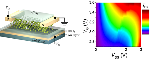
In this work, the NDR effect is demonstrated to be closely related to the conduction type switching of the ambipolar channel under specific electrical field conditions, and is distinct from conventional NDR devices that rely on quantum tunneling. As a result, the NDR device exhibits a high peak current density (34 µA µm−1) and a high operating temperature (330 K).
More importantly, due to the strong coupling between the channel and gate electrode, both the NDR peak current and peak/valley voltages can be effectively modulated by the electrostatic gate. The value of negative output conductance increases with the increasing gate voltages and reaches −204 µS under 3.6 V, which is superior to that obtained using 2D van der Waals heterostructures. The researchers also explored the dependence of NDR and kink characteristics on the temperature and attribute them to the different injection modes of electrons and holes.
In addition, light is demonstrated to be an additional terminal for NDR modulation, which cannot only effectively control the peak current and peak voltages, but also induce NDR in the scenario where dark current shows no NDR characteristics. The photoresponsivity reaches 2.1 × 10⁵ A W−1.
These results could not only provide an important insight into the transport behavior of ambipolar BP transistors, but also contribute to the design of ambipolar-semiconductor-based electrical circuits. In addition, the devices presented here are just based on an individual BP flake and differ strongly from previous heterostructure tunneling devices.
The simplicity of this structure, combined with the recent progress in scalable production of BP films, makes the BP NDR devices promising for practical electronic applications.
Discover Also
Scientists have taken a major step toward a circular carbon economy by developing a long-lasting, economical catalyst that recycles greenhouse gases into ingredients that can be used in fuel, hydrogen gas, and other chemicals. The results could be revolutionary in the effort to reverse global warming, according to the researchers.
Read moreDespite the progress in perovskite device efficiencies, these systems are not fully understood, in particular the frequency- and power-dependence of their response to light. Yu-Hwa Lo and colleagues at the University of California in San Diego (UCSD) now report on systematic investigations of how these devices respond to light for frequencies varying over eight orders of magnitude and power ranging from millions to single photons.
Read more