19 août 2019

[Thin films] – Crystalline GaAs Thin Film Growth on a c-Plane Sapphire Substrate

Accueil > Actualités > [Thin films] – Crystalline GaAs Thin Film Growth on a c-Plane Sapphire Substrate
Flèche contenu
Crystalline AsGa thin film Growth - Codex International

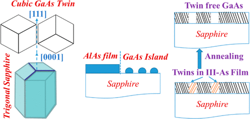
Crystalline zinc blende GaAs has been grown on a trigonal c-plane sapphire substrate by molecular beam epitaxy. The initial stage of GaAs thin film growth has been investigated extensively in this paper. When grown on c-plane sapphire, it takes (111) crystal orientation with twinning as a major problem. Direct growth of GaAs on sapphire results in three-dimensional GaAs islands, almost 50% twin volume, and a weak in-plane correlation with the substrate. Introducing a thin AlAs nucleation layer results in complete wetting of the substrate, better in-plane correlation with the substrate, and reduced twinning to 16%. Further, we investigated the effect of growth temperature, pregrowth sapphire substrate surface treatment, and in-situ annealing on the quality of the GaAs epilayer. We have been able to reduce the twin volume below 2% and an X-ray diffraction rocking curve line width to 223 arcsec. A good quality GaAs on sapphire can result in the implementation of microwave photonic functionality on a photonic chip.

Découvrir
[Nanotechnology] – Spiral dislocation gives 3D topological photonics a robust edge 28 septembre 2022

Researchers from the University of Rostock and Technion Haifa have created the first three-dimensional topological insulator for light. A judiciously placed screw dislocation allows optical signals to wind around the surface of a synthetic lattice while keeping it protected from scattering.
Their discovery has recently been published in the journal Nature (« Photonic topological insulator induced by a dislocation in three dimensions »).

Lire la suite
[Ultra High Vacuum] – The importance of a Sapphire viewport in a HV or UHV 23 février 2020

It is vital for the procedure in-situ to be observed in many high vacuum and ultra-high vacuum (HV/UHV) processes. The challenge is that any optical component must penetrate the hermetically sealed chamber but not compromise the quality of the vacuum.

Lire la suite